Fairchild NC7SZ34 Data Handbook
Summary
The NC7SZ34 is a single buffer from Fairchild’s TinyLogic UHS series, offering ultra-high speed and broad voltage support. This manual covers features, pin configurations, and electrical characteristics, making it ideal for high-performance digital circuits.
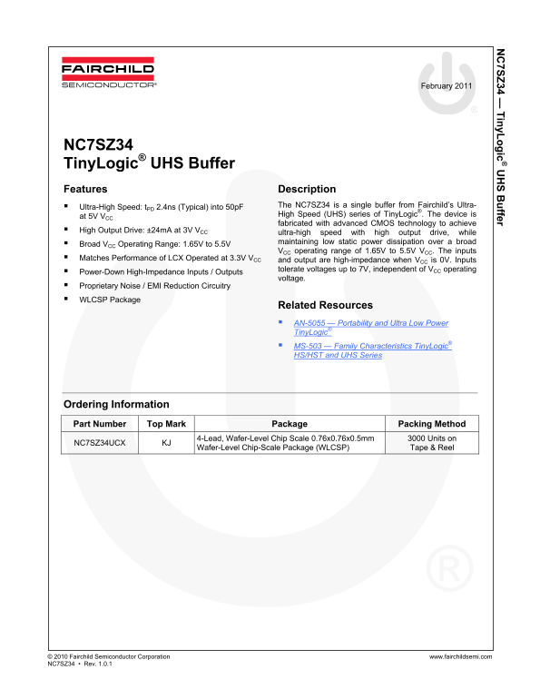
Page 1 Text Content
7S 34 — in y L ic ffer
February 2011
NC7SZ34 Tiny Logic® UHS Buffer Features Description
Ultra-High Speed: t PD 2.4ns (Typical) into 50p F The NC7SZ34 is a single buffer from Fairchild’s Ultra- High Speed (UHS) series of Tiny Logic®. The device is
at 5V VCC
fabricated with advanced CMOS technology to achieve
High Output Drive: ±24m A at 3V VCC
ultra-high speed with high output drive, while Broad VCC Operating Range: 1.65V to 5.5V maintaining low static power dissipation over a broad VCC operating range of 1.65V to 5.5V VCC. The inputs
Matches Performance of LCX Operated at 3.3V VCC and output are high-impedance when VCC is 0V. Inputs
tolerate voltages up to 7V, independent of VCC operating
Power-Down High-Impedance Inputs / Outputs
voltage.
Proprietary Noise / EMI Reduction Circuitry WLCSP Package
Related Resources AN-5055 — Portability and Ultra Low Power Tiny Logic® MS-503 — Family Characteristics Tiny Logic® HS/HST and UHS Series
Ordering Information Part Number Top Mark Package Packing Method
4-Lead, Wafer-Level Chip Scale 0.76x0.76x0.5mm 3000 Units on
NC7SZ34UCX KJ
Wafer-Level Chip-Scale Package (WLCSP) Tape & Reel
© 2010 Fairchild Semiconductor Corporation www.fairchildsemi.com NC7SZ34 • Rev. 1.0.1
Page Summary Contents For Fairchild NC7SZ34 Data Handbook
Manual Details
| Brand | Fairchild |
|---|---|
| Pages | 8 |
| File Size | 609.33 KB |
| Published | June 15, 2026 |
Enter the captcha to get the download link:

Frequently Asked Questions
What is the operating voltage range for the NC7SZ34 buffer?
The operating voltage range is 1.65V to 5.5V.
What is the typical propagation delay?
It has an ultra-high speed of 2.4ns (typical) into 50pF at 5V VCC.
What package does the NC7SZ34 come in?
It comes in a 4-lead Wafer-Level Chip-Scale Package (WLCSP).
What is the maximum DC output current?
The maximum DC output current is ±50mA.
What happens to inputs and outputs when VCC is 0V?
The inputs and outputs become high-impedance when VCC is 0V.