Fairchild MM74C89 Data Handbook
Summary
The MM74C89 is a high-performance 64-Bit, 3-STATE Random Access Memory designed for reliable data storage and system expansion. This manual provides comprehensive technical specifications intended for hardware engineers and circuit designers integrating the component into complex systems. Coverage includes detailed guides on read/write operations, critical timing parameters, wide voltage operating ranges (3.0V to 15V), and advanced electrical characteristics, ensuring precise integration of this low-power, high-immunity memory chip.
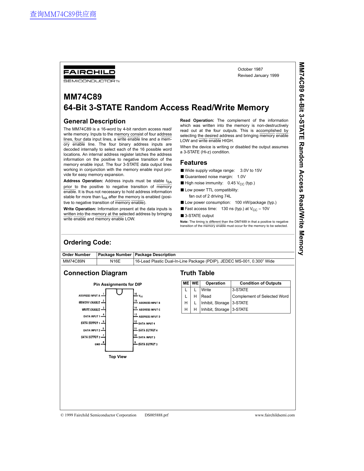
Page 1 Text Content
查询MM74C89供应商
74C 89 64-B it 3-S TA an ccess R ead /W rite M em ry
October 1987 Revised January 1999
MM74C89 64-Bit 3-STATE Random Access Read/Write Memory
Read Operation: The complement of the information
General Description
which was written into the memory is non-destructively
The MM74C89 is a 16-word by 4-bit random access read/
read out at the four outputs. This is accomplished by
write memory. Inputs to the memory consist of four address
selecting the desired address and bringing memory enable
lines, four data input lines, a write enable line and a mem-
LOW and write enable HIGH.
ory enable line. The four binary address inputs are
When the device is writing or disabled the output assumes
decoded internally to select each of the 16 possible word
a 3-STATE (Hi-z) condition.
locations. An internal address register latches the address information on the positive to negative transition of the
memory enable input. The four 3-STATE data output lines Features
working in conjunction with the memory enable input pro- Wide supply voltage range: 3.0V to 15V vide for easy memory expansion.
Guaranteed noise margin: 1.0V
Address Operation: Address inputs must be stable t SA
High noise immunity: 0.45 VCC (typ.)
prior to the positive to negative transition of memory
Low power TTL compatibility:
enable. It is thus not necessary to hold address information
stable for more than t HA after the memory is enabled (posi- fan out of 2 driving 74L tive to negative transition of memory enable). Low power consumption: 100 n W/package (typ.) Write Operation: Information present at the data inputs is Fast access time: 130 ns (typ.) at VCC = 10V
written into the memory at the selected address by bringing
3-STATE output
write enable and memory enable LOW.
Note: The timing is different than the DM7489 in that a positive to negative transition of the memory enable must occur for the memory to be selected.
Ordering Code: Order Number Package Number Package Description MM74C89N N16E 16-Lead Plastic Dual-In-Line Package (PDIP), JEDEC MS-001, 0.300” Wide
Connection Diagram Truth Table ME WE Operation Condition of Outputs
Pin Assignments for DIP
Write 3-STATE Read Complement of Selected Word Inhibit, Storage 3-STATE Inhibit, Storage 3-STATE
Top View
© 1999 Fairchild Semiconductor Corporation DS005888.prf www.fairchildsemi.com
Page Summary Contents For Fairchild MM74C89 Data Handbook
Manual Details
| Brand | Fairchild |
|---|---|
| Pages | 6 |
| File Size | 58.74 KB |
| Published | July 07, 2026 |
Enter the captcha to get the download link:

Frequently Asked Questions
What is the device's operating temperature range?
The operating temperature range is −40°C to +85°C.
What voltage levels are supported for operation?
It supports an operating supply voltage range of 3.0V to 15V.
How must the memory be selected during setup or operation?
The selection requires a positive-to-negative transition on the memory enable input.
What is the typical access time for this data memory?
The device has a fast, typical address access time of 130 ns at V = 10V.