Fairchild FST3125 4-Bit Bus Switch Data Handbook
Summary
This highly reliable, CMOS TTL bus switch provides four high-speed electrical connections facilitating robust data transfer between two ports (A and B). Designed for optimal signal integrity, it features minimal propagation delay and zero bounce in flow-through mode. The documentation details comprehensive technical specifications, including various package types (SOIC, QSOP, TSSOP), electrical characteristics, operating limits, and pin layouts, making it essential for electronics engineers designing precision digital circuits requiring dependable bus switching.
Page 1 Text Content
FST3125 — 4-B it B us Sw itch
March 2008
FST3125 — 4-Bit Bus Switch Features Description
4Ω Switch Connection between Two Ports Fairchild switch FST3125 provides four high-speed CMOS TTL-compatible bus switches. The low on
Minimal Propagation Delay through the Switch
resistance of the switch allows inputs to be connected to outputs without adding propagation delay or
Low ICC
generating additional ground bounce noise.
Zero Bounce in Flow-through Mode
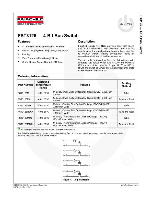
The device is organized as four one1-bit switches with
Control Inputs Compatible with TTL Level
separate /OE inputs. When /OE is LOW, the switch is ON and port A is connected to port B. When /OE is HIGH, the switch is OPEN and a high-impedance state exists between the two ports.
Ordering Information
Operating
Part Number Temperature Package Packing
Method
Range
FST3125M -40 to 85°C 14-Lead, Small Outline Integrated Circuit (SOIC) 0.150 inch
Narrow Tube
FST3125MX -40 to 85°C 14-Lead, Small Outline Integrated Circuit (SOIC) 0.150 inch
Narrow Tape and Reel
FST3125QSC -40 to 85°C 16-Lead, Quarter Size Outline Package (QSOP) MO-137
0.150 inch Wide Tube
FST3125QSCX -40 to 85°C 16-Lead, Quarter Size Outline Package (QSOP) MO-137
0.150 inch Wide Tape and Reel
FST3125MTC -40 to 85°C 14-Lead, Thin Shrink Small Outline Package (TSSOP)
MO-153, 4mm Wide Tube
FST3125MTCX -40 to 85°C 14-Lead, Thin Shrink Small Outline Package (TSSOP)
MO-153, 4mm Wide Tape and Reel
All packages are lead free per JEDEC: J-STD-020B standard. The Fairchild switch family derives from and embodies Fairchild’s proven switch technology used for several years in its 74LVX3L384 (FST3384) bus switch product.
Figure 1. Logic Diagram
© 2005 Fairchild Semiconductor Corporation www.fairchildsemi.com FST3125 • Rev. 1.0.3
Page Summary Contents For Fairchild FST3125 4-Bit Bus Switch Data Handbook
Manual Details
| Brand | Fairchild |
|---|---|
| Pages | 9 |
| File Size | 440.57 KB |
| Published | June 20, 2026 |
Enter the captcha to get the download link:

Frequently Asked Questions
How does this bus switch operate?
The switch connects Port A to Port B when /OE is LOW, and enters a high-impedance state when /OE is HIGH.
What are the recommended operating voltage ranges?
VCC/VEE should be between 4.0 V and 5.5 V, with input/output voltages also restricted to 0 V to 5.5 V.
Does it minimize electrical noise and delays?
Yes, it offers minimal propagation delay and low ICC, which helps in reducing ground bounce noise.
What are the available package options for this chip?
It is available in packaging types including SOIC, QSOP, TSSOP, and their Tape and Reel variations.