Fairchild FSQ100 Data Handbook
Summary
This integrated switching regulator is a compact solution for high-efficiency, off-line Switch-Mode Power Supplies (SMPS). It combines core components—including a VDMOS SenseFET and PWM modulator—into a single chip, drastically reducing component count while maximizing reliability. The manual provides comprehensive design guidelines and support for implementing flyback converters, making it ideal for engineers developing adapters and power sources for mobile phone chargers, PCs, monitors, and other auxiliary electronic equipment.
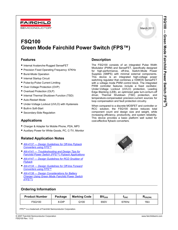
Page 1 Text Content
100 — reen e F airch ild er S itch (F
March 2011
FSQ100 Green Mode Fairchild Power Switch (FPS™)
Features Description
Internal Avalanche-Rugged Sense FET The FSQ100 consists of an integrated Pulse Width Modulator (PWM) and Sense FET, specifically designed
Precision Fixed Operating Frequency: 67KHz
for high-performance, off-line, Switch-Mode Power Burst-Mode Operation Supplies (SMPS) with minimal external components. This device is an integrated high-voltage power
Internal Startup Circuit
switching regulator that combines a VDMOS Sense FET
Pulse-by-Pulse Current Limiting with a voltage mode PWM control block. The integrated
PWM controller features include a fixed oscillator,
Over-Voltage Protection (OVP)
Under-Voltage Lockout (UVLO) protection, Leading
Overload Protection (OLP)
Edge Blanking (LEB), an optimized gate turn-on/turn-off Internal Thermal Shutdown Function (TSD) driver, Thermal Shutdown (TSD) protection, and temperature-compensated precision-current sources for
Auto-Restart Mode
loop compensation and fault protection circuitry.
Under-Voltage Lockout (UVLO) with Hysteresis
When compared to a discrete MOSFET and controller or
Built-in Soft-Start RCC solution, the FSQ100 device reduces total
component count and design size and weight, while
Secondary-Side Regulation
increasing efficiency, productivity, and system reliability. This device provides a basic platform well suited for
Applications cost-effective flyback converters. Charger & Adapter for Mobile Phone, PDA, MP3 Auxiliary Power for White Goods, PC, C-TV, Monitor
Related Application Notes AN-4137 — Design Guidelines for Off-line Flyback Converters using FPS™ AN-4141 — Troubleshooting and Design Tips for Fairchild Power Switch (FPS™) Flyback Applications AN-4147 — Design Guidelines for RCD Snubber of Flyback AN-4134 — Design Guidelines for Off-line Forward Converters using FPS™ AN-4138 — Design Considerations for Battery Charger Using Green Mode Fairchild Power Switch (FPS™)
Ordering Information
Product Number Package Marking Code BVDSS f OSC RDS(ON) FSQ100 8-DIP Q100 650V 67KHz 16Ω
FPS™ is a trademark of Fairchild Semiconductor Corporation.
© 2007 Fairchild Semiconductor Corporation www.fairchildsemi.com FSQ100 Rev. 1.0.2
Page Summary Contents For Fairchild FSQ100 Data Handbook
Manual Details
| Brand | Fairchild |
|---|---|
| Pages | 12 |
| File Size | 799.99 KB |
| Published | June 15, 2026 |
Enter the captcha to get the download link:

Frequently Asked Questions
What protections does the FSQ100 integrate into its PWM controller?
It includes Over-Voltage Protection (OVP), Under-Voltage Lockout (UVLO), Overload Protection (OLP), and Thermal Shutdown (TSD) protection.
What applications is this device best suited for?
It is well suited for cost-effective flyback converters, such as chargers/adapters for phones or auxiliary power for white goods and monitors.
How can I change the burst mode operation frequency?
You can adjust it by increasing a feedback gain capacitor (C) and decreasing a feedback gain resistor (R).
What is the maximum voltage capability of the drain pins?
The drain pins are capable of switching a maximum of 650V.