Fairchild FSD146MRBN Data Handbook
Summary
This advanced power switch is an IC solution designed for high-efficiency, reliable power supplies in consumer electronics like LCD monitors, set-top boxes, and DVD players. It features integrated PWM control, soft burst operation, and comprehensive protection circuits (e.g., Overload/Over-Voltage Protection). The manual provides full technical specifications, application circuit diagrams, operational guides, and pin definitions, making it an essential resource for electrical engineers and power electronics designers working on cost-effective, low-power Standby Mode devices that require minimal external components.
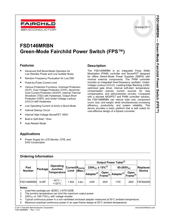
Page 1 Text Content
6M reen -M e F airch ild er S itch (F
October 2011
FSD146MRBN Green-Mode Fairchild Power Switch (FPS™)
Features Description
Advanced Soft Burst-Mode Operation for The FSD146MRBN is an integrated Pulse Width Low Standby Power and Low Audible Noise Modulation (PWM) controller and Sense FET designed for offline Switch-Mode Power Supplies (SMPS) with
Random Frequency Fluctuation for Low EMI
minimal external components. The PWM controller Pulse-by-Pulse Current Limit includes an integrated fixed-frequency oscillator, Under- Voltage Lockout (UVLO), Leading-Edge Blanking (LEB),
Various Protection Functions: Overload Protection
optimized gate driver, internal soft-start, temperature-
(OLP), Over-Voltage Protection (OVP), Abnormal
compensated precise current sources for loop
Over-Current Protection (AOCP), Internal Thermal
compensation, and self-protection circuitry. Compared
Shutdown (TSD) with Hysteresis, Output-Short
with a discrete MOSFET and PWM controller solution,
Protection (OSP), and Under-Voltage Lockout
the FSD146MRBN can reduce total cost, component
(UVLO) with Hysteresis
count, size, and weight; while simultaneously increasing Low Operating Current (0.4m A) in Burst Mode efficiency, productivity, and system reliability. This device provides a basic platform that is well suited for
Internal Startup Circuit
cost-effective design of a flyback converter.
Internal High-Voltage Sense FET: 650V Built-in Soft-Start: 15ms Auto-Restart Mode
Applications Power Supply for LCD Monitor, STB, and DVD Combination
Ordering Information
Output Power Table(2)
Operating
Part Current RDS(ON) 230VAC ± 15%(3) 85-265VAC Replaces
Package Junction
Number Limit (Max.) Device
Temperature Open Open
Adapter(4) Adapter(4)
Frame(5) Frame(5)
FSD146MRBN 8-DIP 1.50A 2.6 23W 35W 17W 26W FSFM260N
Notes: 1. Lead-free package per JEDEC J-STD-020B. 2. The junction temperature can limit the maximum output power. 3. 230VAC or 100/115VAC with voltage doubler. 4. Typical continuous power in a non-ventilated enclosed adapter measured at 50C ambient temperature. 5. Maximum practical continuous power in an open-frame design at 50C ambient temperature. © 2011 Fairchild Semiconductor Corporation www.fairchildsemi.com FSD146MRBN • Rev. 1.0.0
Page Summary Contents For Fairchild FSD146MRBN Data Handbook
Manual Details
| Brand | Fairchild |
|---|---|
| Pages | 16 |
| File Size | 632.20 KB |
| Published | June 06, 2026 |
Enter the captcha to get the download link:

Frequently Asked Questions
What is the Soft-Start function duration on this device?
The internal soft-start time is 15ms.
How does Overload Protection trigger on the FSD146MRBN?
Overload protection triggers when the Feedback (FB) pin voltage reaches 7.0V, causing the FPS™ to shut down.
What are the built-in protective functions included in the chip?
It includes UVLO, OVP, OLP, AOCP, TSD, and OSP circuitry.
What is the operating temperature range for the FSD146MRBN?
The recommended operating junction temperature range is -40°C to +125°C.