Fairchild FQPF33N10L Data Handbook
Summary
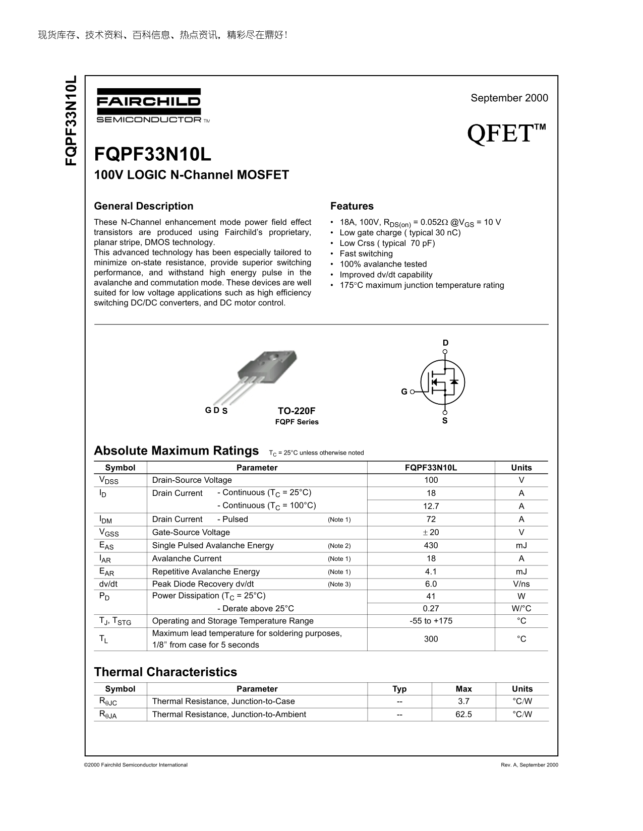
This technical datasheet details the FQPF33N10L, a high-efficiency N-Channel MOSFET designed for demanding low-voltage switching applications. Featuring advanced planar stripe DMOS technology, this transistor provides superior fast switching, low on-resistance (Rds(on)), and robust performance under high energy pulses. The comprehensive manual covers absolute maximum ratings, detailed electrical characteristics, thermal properties, and dynamic curves. It is the ideal component for engineers developing high-efficiency DC/DC converters and precise DC motor control systems.
Page 1 Text Content
September 2000
QFETTM
FQPF33N10L 100V LOGIC N-Channel MOSFET General Description Features These N-Channel enhancement mode power field effect 18A, 100V, RDS(on) = 0.052Ω @VGS = 10 V transistors are produced using Fairchild’s proprietary, Low gate charge ( typical 30 n C) planar stripe, DMOS technology. Low Crss ( typical 70 p F) This advanced technology has been especially tailored to Fast switching minimize on-state resistance, provide superior switching 100% avalanche tested performance, and withstand high energy pulse in the
Improved dv/dt capability
avalanche and commutation mode. These devices are well
175°C maximum junction temperature rating
suited for low voltage applications such as high efficiency switching DC/DC converters, and DC motor control.
SD TO-220F
FQPF Series
Absolute Maximum Ratings TC = 25°C unless otherwise noted Symbol Parameter FQPF33N10L Units VDSS Drain-Source Voltage ID Drain Current - Continuous (TC = 25°C)
- Continuous (TC = 100°C) 12.7
IDM Drain Current - Pulsed (Note 1) VGSS Gate-Source Voltage ± 20 EAS Single Pulsed Avalanche Energy (Note 2) m J IAR Avalanche Current (Note 1) EAR Repetitive Avalanche Energy (Note 1) 4.1 m J
dv/dt Peak Diode Recovery dv/dt (Note 3) 6.0 V/ns
PD Power Dissipation (TC = 25°C)
- Derate above 25°C 0.27 W/°C
TJ, TSTG Operating and Storage Temperature Range -55 to +175 °C
Maximum lead temperature for soldering purposes,
TL °C
1/8" from case for 5 seconds
Thermal Characteristics Symbol Parameter Typ Max Units RθJC Thermal Resistance, Junction-to-Case 3.7 °C/W RθJA Thermal Resistance, Junction-to-Ambient 62.5 °C/W
©2000 Fairchild Semiconductor International Rev. A, September 2000
Page Summary Contents For Fairchild FQPF33N10L Data Handbook
Manual Details
| Brand | Fairchild |
|---|---|
| Pages | 8 |
| File Size | 672.94 KB |
| Published | July 12, 2026 |
Enter the captcha to get the download link:

Frequently Asked Questions
这是什么类型的功率 MOSFET?
这是一款N沟道增强型功率场效应晶体管。
该器件适用于哪些低压应用场景?
它适用于高效率开关式DC/DC转换器和直流电机控制等低电压应用。
最大连续漏极电流是多少?
在25°C室温下,其最大的连续漏极电流(IDSS)可达18 A。
该芯片的最大工作结温是多少?
该器件的最大结温额定值为175°C。