Fairchild FDP603AL FDB603AL Data Handbook
Summary
The FDP603AL/FDB603AL is a high-performance N-Channel Logic Level MOSFET optimized for low voltage, high-efficiency power switching applications. Featuring extremely low on-state resistance and robust transient handling, this device is ideal for powering DC/DC converters and high-power management systems. This technical guide provides comprehensive electrical characteristics, thermal ratings, and complex operational data—including detailed performance curves and specifications—making it an essential resource for professional power electronics engineers and circuit designers.
Page 1 Text Content
查询FDB603AL供应商
April 1998
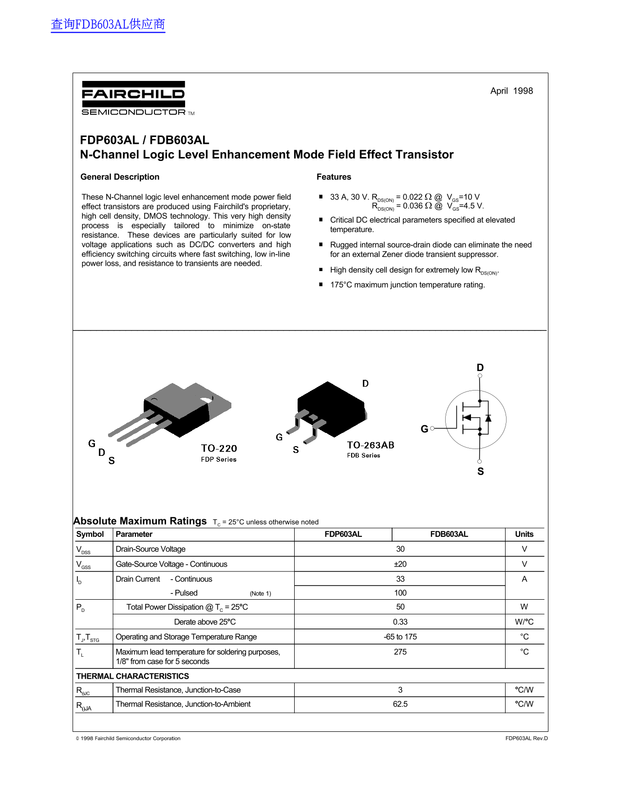
FDP603AL / FDB603AL N-Channel Logic Level Enhancement Mode Field Effect Transistor General Description Features
These N-Channel logic level enhancement mode power field 33 A, 30 V. RDS(ON) = 0.022 Ω @ VGS=10 V
effect transistors are produced using Fairchild's proprietary, RDS(ON) = 0.036 Ω @ VGS=4.5 V.
high cell density, DMOS technology. This very high density
Critical DC electrical parameters specified at elevated
process is especially tailored to minimize on-state
temperature.
resistance. These devices are particularly suited for low voltage applications such as DC/DC converters and high Rugged internal source-drain diode can eliminate the need efficiency switching circuits where fast switching, low in-line for an external Zener diode transient suppressor. power loss, and resistance to transients are needed.
High density cell design for extremely low RDS(ON).
175°C maximum junction temperature rating.
Absolute Maximum Ratings TC = 25°C unless otherwise noted Symbol Parameter FDP603AL FDB603AL Units
VDSS Drain-Source Voltage
VGSS Gate-Source Voltage - Continuous ±20
ID Drain Current - Continuous 33 - Pulsed (Note 1)
PD Total Power Dissipation @ TC = 25°C 50
Derate above 25°C 0.33 W/°C
TJ,TSTG Operating and Storage Temperature Range -65 to 175 °C
TL Maximum lead temperature for soldering purposes, °C
1/8" from case for 5 seconds
THERMAL CHARACTERISTICS
RθJC Thermal Resistance, Junction-to-Case °C/W RθJA Thermal Resistance, Junction-to-Ambient 62.5 °C/W
© 1998 Fairchild Semiconductor Corporation FDP603AL Rev.D
Page Summary Contents For Fairchild FDP603AL FDB603AL Data Handbook
Manual Details
| Brand | Fairchild |
|---|---|
| Pages | 4 |
| File Size | 412.75 KB |
| Published | July 15, 2026 |
Enter the captcha to get the download link:

Frequently Asked Questions
What is the maximum drain current this transistor can handle?
The continuous Drain Current (ID) rating is 33 A.
How much power can it dissipate at room temperature?
Total Power Dissipation at T=25°C is listed as 50 W.
What are the device's operating temperature limits?
The Operating and Storage Temperature Range is from -65 to 175 °C.
How does the on-resistance change with temperature?
The static Drain-Source On-Resistance (RDS(ON)) increases as junction temperature rises, demonstrating sensitivity at higher temps.