Fairchild FDD8880 Product Manual
Summary
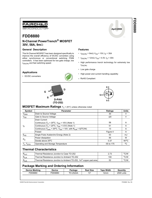
N-Channel PowerTrench MOSFET in D-PAK (TO-252) package for DC/DC converters. The FDD8880 delivers 30V with 58A continuous current and 9mohm on-resistance at 10V gate drive. Optimized for low gate charge and fast switching, it improves efficiency in synchronous and conventional PWM topologies. Uses high-performance trench technology. Key specs: 1.1V threshold, 1720pF input capacitance, 10ns/8ns rise/fall. RoHS compliant, -55 to 175C. Targeted at power electronics engineers.
Page 1 Text Content
April 2008
FDD8880 tm N-Channel Power Trench® MOSFET 30V, 58A, 9mΩ General Description Features This N-Channel MOSFET has been designed specifically to r DS(ON) = 9mΩ, VGS = 10V, ID = 35A improve the overall efficiency of DC/DC converters using
either synchronous or conventional switching PWM r DS(ON) = 12mΩ, VGS = 4.5V, ID = 35A
controllers. It has been optimized for low gate charge, low
High performance trench technology for extremely low
r DS(ON) and fast switching speed.
r DS(ON)
Low gate charge
Applications
High power and current handling capability
DC/DC converters
• Ro HS Compliant
TO-252D-PAK (TO-252)
MOSFET Maximum Ratings TC = 25°C unless otherwise noted Symbol Parameter Ratings Units VDSS Drain to Source Voltage VGS Gate to Source Voltage ±20
Drain Current
AContinuous (TC = 25o C, VGS = 10V) (Note 1)
ID Continuous (TC = 25o C, VGS = 4.5V) (Note 1)
Continuous (Tamb = 25o C, VGS = 10V, with RθJA = 52o C/W) Pulsed Figure 4
EAS Single Pulse Avalanche Energy (Note 2) m J
Power dissipation
Derate above 25o C 0.37 W/o C
TJ, TSTG Operating and Storage Temperature -55 to 175
Thermal Characteristics
RθJC Thermal Resistance Junction to Case TO-252 2.73
RθJA Thermal Resistance Junction to Ambient TO-252
RθJA Thermal Resistance Junction to Ambient TO-252, 1in2 copper pad area
Package Marking and Ordering Information Device Marking Device Package Reel Size Tape Width Quantity FDD8880 FDD8880 TO-252AA 13” 12mm 2500 units
2008 Fairchild Semiconductor Corporation FDD8880 Rev. B3
Page Summary Contents For Fairchild FDD8880 Product Manual
Manual Details
| Brand | Fairchild |
|---|---|
| Pages | 11 |
| File Size | 498.90 KB |
| Published | June 17, 2026 |
Enter the captcha to get the download link:

Frequently Asked Questions
What is the maximum continuous drain current of the FDD8880 at 25°C with 10V gate-source voltage?
58A, limited to 35A by the package.
What are the typical on-resistance values for the FDD8880?
9mΩ at Vgs=10V, 12mΩ at Vgs=4.5V, both at Id=35A.
What is the operating temperature range of the FDD8880?
-55°C to 175°C for both operating and storage.
What package does the FDD8880 use?
It uses the TO-252 (D-PAK) surface mount package.