Fairchild FAN5358 Product Manual
Summary
This high-efficiency synchronous buck regulator is engineered for robust power management in portable electronics, including smartphones, data cards, and ultra-mobile PCs. Offering stable voltage outputs (1.0–1.8V) from a wide 2.7V to 5.5V input range while maintaining over 80% efficiency, the FAN5358 ensures reliable power delivery in demanding mobile applications. This manual provides complete technical documentation, including detailed operating specifications, component selection guidelines, pin configurations, and thermal parameters necessary for optimal system integration into tight-space product designs.
Page 1 Text Content
5358 — 2M z, 500m , S 70 S yn ch ro s B ck R eg lato
August 2011
FAN5358 2MHz, 500m A, SC70 Synchronous Buck Regulator Features Description
2MHz Nominal-Frequency Operation The FAN5358 is a step-down switching voltage regulator that delivers a fixed output from an input voltage supply of 2.7V to
25µA Typical Quiescent Current
5.5V. Using a proprietary architecture with synchronous 500m A Output Current Capability rectification, the device is capable of delivering 500m A and maintaining a very high efficiency of over 80% at load currents
2.7V to 5.5V Input Voltage Range
as low as 1m A. The regulator operates at a nominal frequency of 2MHz, which reduces the value of the external components
1.0 to 1.8V Fixed Output Voltages
to as low as 2.2H for the output inductor and 4.7µF for the
Low Ripple, Light-Load PFM Mode
output capacitor.
Internal Soft-Start
At moderate and light loads, pulse frequency modulation is Input Under-Voltage Lockout (UVLO) used to operate the device in power-save mode with a typical quiescent current of 25µA. Even with such a low quiescent
Thermal Shutdown and Overload Protection
current, the part exhibits excellent transient response during 6-lead 2 x 2.2mm SC70 large load swings. In shutdown mode, the supply current drops below 1µA, reducing power consumption. FAN5358 is available in a 6-lead SC70 package.
Applications Cell Phones, Smart Phones 3G, 4G, Wi Fi®, Wi MAX™, and Wi Bro® Data Cards Netbooks®, Ultra-Mobile PCs
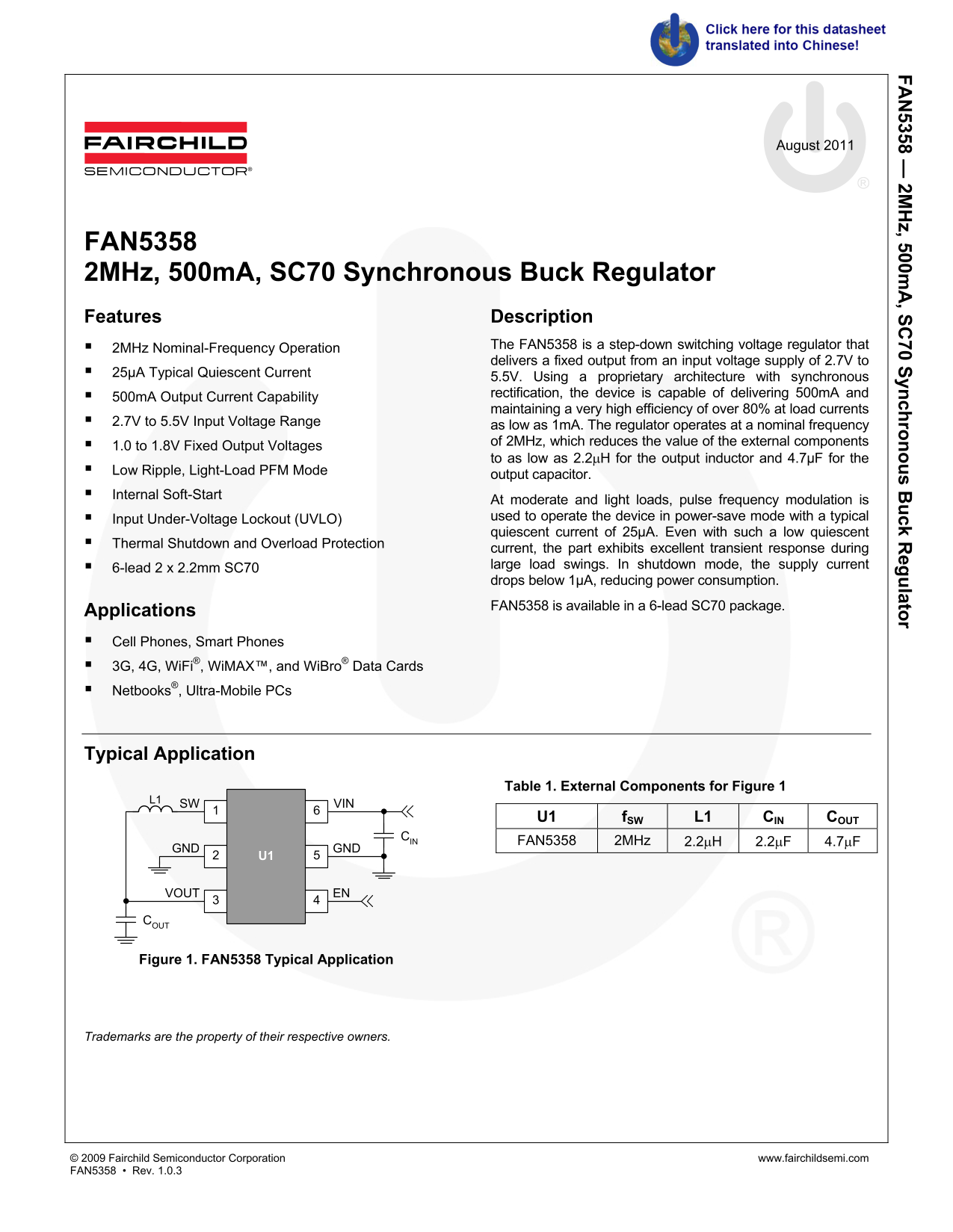
Typical Application
Table 1. External Components for Figure 1
L1 SW VIN
U1 f SW L1 CIN COUT
FAN5358 2MHz 2.2H 2.2F 4.7F
GND GND
VOUT EN
Figure 1. FAN5358 Typical Application
Trademarks are the property of their respective owners.
© 2009 Fairchild Semiconductor Corporation www.fairchildsemi.com FAN5358 • Rev. 1.0.3
Page Summary Contents For Fairchild FAN5358 Product Manual
Manual Details
| Brand | Fairchild |
|---|---|
| Pages | 13 |
| File Size | 1.01 MB |
| Published | July 16, 2026 |
Enter the captcha to get the download link:

Frequently Asked Questions
What is the maximum continuous output current?
The device is capable of delivering up to 500mA of output current.
What external components are required for operation?
It requires an inductor (L1) of 2.2µH, an input capacitor (C IN) of 2.2µF, and an output capacitor (C OUT) of 4.7µF.
How does the device achieve low power consumption at light loads?
It uses Pulse Frequency Modulation (PFM) mode to operate in a power-save state with a typical quiescent current of 25µA.
What voltage level is required for normal operation/enablement?
The device must have a voltage on the EN pin that is greater than 1.2V to be enabled and operational.