Fairchild FDD8778 FDU8778 Specifications Manual
Summary
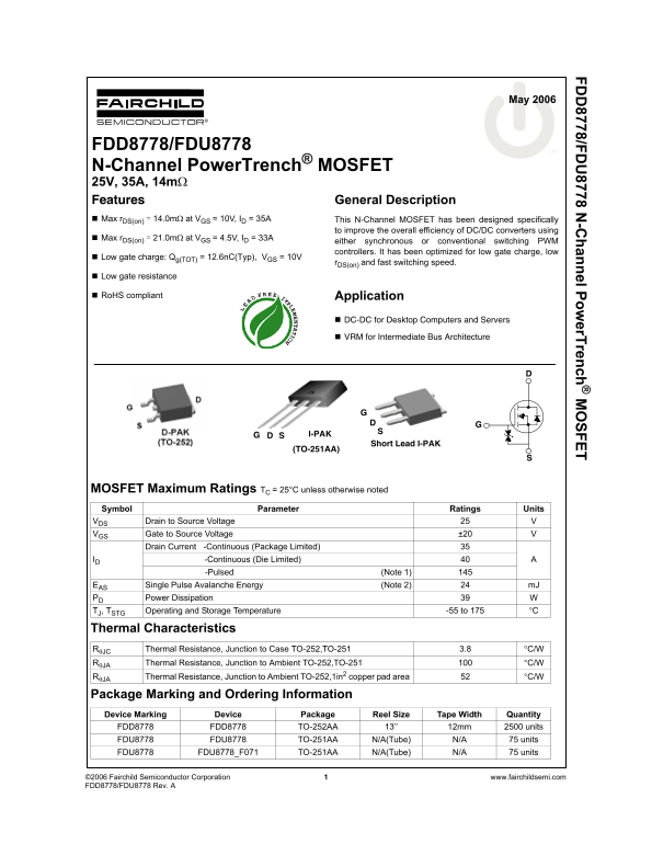
The N O I T A T® FDD8778/FDU8778 is a high-efficiency N-Channel PowerTrench MOSFET engineered for demanding DC/DC converter applications. Ideal for powering professional components, this device excels in VRMs used in servers and desktop computer architectures due to its low on-resistance (max 14mΩ) and optimized gate charge for fast switching. This technical manual provides detailed specifications, covering electrical characteristics, thermal performance data, maximum operating ratings up to 175°C, and precise package information required for circuit design and reliable integration into power systems.
Page 1 Text Content
FD 8778/FD 8778 N -C hannel Pow er Tren ch SFET
May 2006
tm FDD8778/FDU8778
N-Channel Power Trench® MOSFET 25V, 35A, 14mΩ Features General Description Max r DS(on) = 14.0mΩ at VGS = 10V, ID = 35A This N-Channel MOSFET has been designed specifically
to improve the overall efficiency of DC/DC converters using
Max r DS(on) = 21.0mΩ at VGS = 4.5V, ID = 33A
either synchronous or conventional switching PWM controllers. It has been optimized for low gate charge, low
Low gate charge: Qg(TOT) = 12.6n C(Typ), VGS = 10V
r DS(on) and fast switching speed.
Low gate resistance
Ro HS compliant FR EE
Application
DC-DC for Desktop Computers and Servers
VRM for Intermediate Bus Architecture
TA TIO
I-PAK
Short Lead I-PAK
(TO-251AA)
MOSFET Maximum Ratings TC = 25°C unless otherwise noted Symbol Parameter Ratings Units VDS Drain to Source Voltage
VGS Gate to Source Voltage ±20 Drain Current -Continuous (Package Limited)
ID A -Continuous (Die Limited)
-Pulsed (Note 1) EAS Single Pulse Avalanche Energy (Note 2) m J PD Power Dissipation 39 TJ, TSTG Operating and Storage Temperature -55 to 175 °C
Thermal Characteristics
RθJC Thermal Resistance, Junction to Case TO-252,TO-251 3.8 °C/W RθJA Thermal Resistance, Junction to Ambient TO-252,TO-251 °C/W RθJA Thermal Resistance, Junction to Ambient TO-252,1in2 copper pad area 52 °C/W
Package Marking and Ordering Information Device Marking Device Package Reel Size Tape Width Quantity FDD8778 FDD8778 TO-252AA 13’’ 12mm 2500 units FDU8778 FDU8778 TO-251AA N/A(Tube) N/A 75 units FDU8778 FDU8778_F071 TO-251AA N/A(Tube) N/A 75 units
©2006 Fairchild Semiconductor Corporation www.fairchildsemi.com1 FDD8778/FDU8778 Rev. A
Page Summary Contents For Fairchild FDD8778 FDU8778 Specifications Manual
Manual Details
| Brand | Fairchild |
|---|---|
| Pages | 6 |
| File Size | 358.35 KB |
| Published | May 28, 2026 |
Enter the captcha to get the download link:

Frequently Asked Questions
Can this MOSFET be used in life support devices?
No, Fairchild’s products are not authorized for use as critical components in life support unless you have express written approval.
What applications is the FDD8778/FDU8778 optimized for?
It is designed for improving DC/DC converters efficiency, including VRMs and use in desktop computers and servers.
How low can the component's drain-source on resistance be?
The maximum $R_{DS(on)}$ reported is 14.0 mΩ at V=10V and I=35A.
What thermal resistance values must I consider when cooling this device?
For TO-252, the junction to case ($ heta_{JC}$) is 3.8 °C/W, while the junction to ambient ($ heta_{JA}$) is 100 °C/W.