# A B C D E F G H I J K L M N O P Q R S T U V W X Y Z

Fairchild AN4138 Specifications Manual

Summary

Engineers designing power solutions will find this guide invaluable. This technical manual provides a detailed, step-by-step procedure for optimizing the design of high-efficiency battery chargers using Fairchild Power Switches (FPS). It guides users through every stage—from defining system specifications and selecting components like transformers to calculating optimal capacitor values and achieving maximum reliability. Perfect for professionals building compact, low-cost charging systems for portable electronics.
📄 Preview PAGE OF 20

Page 1 Text Content

www.fairchildsemi.com

Application Note AN4138 Design Considerations for Battery Charger Using Green Mode Fairchild Power Switch (FPSTM)

Abstract The step-by-step design procedure described in this paper will help engineers design battery chargers more easily. In

This application note presents practical design consider-

order to make the design process more efficient, a software

ations for battery chargers employing Green Mode FPS

design tool, FPS design assistant that contains all the

(Fairchild Power Switch). It includes designing the

equations described in this paper is also provided. The

transformer and output filter, selecting the components and

design procedure is verified through an experimental

implementing constant current / constant voltage control.

prototype converter.

DR LP

Bridge rectifier

VDC CO VO

diode Rsn Csn Vsn CP

Np NS

Vbias

Drain

AC line

ref IO

FB Vcc

Current

Ra Da

Controller

Ca Na

ref VO

Voltage Controller

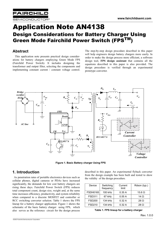
Figure 1. Basic Battery charger Using FPS

1. Introduction described in this paper. An experimental flyback converter from the design example has been built and tested to show

As penetration rates of portable electronics devices such as

the validity of the design procedure.

cellular phones, digital cameras or PDAs have increased significantly, the demands for low cost battery chargers are

Device Switching Current Rdson (typ.)

rising these days. Fairchild Power Switch (FPS) reduces

frequency limit

total component count, design size, weight and, at the same

FSDH0165 100 k Hz 0.35 A 15.6 Ω

time increases efficiency, productivity, and system reliability

FSD311 67 k Hz 0.55 A 14 Ω

when compared to a discrete MOSFET and controller or RCC switching converter solution. Table 1 shows the FPS FSD200 134 k Hz 0.32 A 28 Ω lineup for a battery charger application. Figure 1 shows the

FSD210 134 k Hz 0.32 A 28 Ω

schematic of the basic battery charger using FPS, which

also serves as the reference circuit for the design process Table 1. FPS lineup for a battery charger

Rev. 1.0.0

©2003 Fairchild Semiconductor Corporation

Page Summary Contents For Fairchild AN4138 Specifications Manual

Page 1 www.fairchildsemi.com Application Note AN4138 Design Considerations for Battery Charger Using Green Mode Fairchild Power Switch (FPSTM) Abstract The step-by-step design procedure described in this pap...
Page 2 AN4138 APPLICATION NOTE 2. Step-by-step Design Procedure In this section, a design procedure is presented using the schematic of Figure 1 as a reference. Figure 2 illustrates the design flow chart. Th...
Page 3 APPLICATION NOTE AN4138 (3) STEP-3 : Determine the reflected output voltage (VRO). When the MOSFET in the FPS is turned off, the input voltage (VDC) together with the output voltage reflected to Lm th...
Page 4 AN4138 APPLICATION NOTE condition. Therefore, Lm is obtained in this condition as (5) STEP-5 : Choose the proper FPS considering input VDC Dmax⋅( power and peak drain current. Lm (6) 2Pinfs KRF With t...
Page 5 APPLICATION NOTE AN4138 Fl ux en sit (m T) Vcc* VFa+ agnetization Curves (typical) Na Ns1⋅ turns( 13( aterial :PC40 Vo VF+ where Vcc* is the nominal value of the supply voltage of the FPS device, and ...
Page 6 AN4138 APPLICATION NOTE long (>1m). When the wire is short with a small number of turns, a current density of 6-10 A/mm2 is also acceptable. Schottky Barrier Diode Avoid using wire with a diameter ...
Page 7 APPLICATION NOTE AN4138 peak) is obtained as cycle. The snubber capacitor used should be ceramic or a input voltage and full load condition (Ids2 material that offers low ESR. Electrolytic or tantalum...
Page 8 AN4138 APPLICATION NOTE In the snubber design in this section, neither the lossy temperature stability are a key factor, the op amp current discharge of the inductor nor stray capacitance is considere...
Page 9 APPLICATION NOTE AN4138 where Vo is the output voltage, VOP is opto-diode forward voltage drop, which is typically 1V and IFB is the feedback current of FPS. With IFB=0.25m A (FSD210), Rd and Rbias IC...
Page 10 AN4138 APPLICATION NOTE (36), the resistance of the thermistor at 75°C to keep the same output current is given by NTC thermistor 103Χ2 from DSC is chosen for the compen- sation, whose resistance is 1...
Page 11 APPLICATION NOTE AN4138 sense 0.2 Ω IO 0.1u F 0.8A VR EF=2.5V LM 358A 100kΩ PS 1N LM 358B Figure 15. CC/CV control using OP amp and shunt regulator ©2003 Fairchild Semiconductor Corporation
Page 12 AN4138 APPLICATION NOTE - Summary of symbols - Aw : Winding window area of the core in mm2 Ae : Cross sectional area of the core in mm2 Bsat : Saturation flux density in tesla. Co : Output capacitor D...
Page 13 APPLICATION NOTE AN4138 Design example using FPS Design Assistant Output Ripple Device Application Output voltage (Max Current)Input voltage Power spec 5.2V (0.65A)85V-265VAC3.4WFSD210Battery 5% charg...
Page 14 AN4138 APPLICATION NOTE 5. Choose the proper FPS considering the input power and current limit Typical current limit of FPS (Iover) 0.32 Minimum Iover considering tolerance of 12% 0.28 0.23 6. Determi...
Page 15 APPLICATION NOTE AN4138 10. Determine the output capacitor Co(n) RC(n) Icap(n) ΔVo(n) 1st output capacitor u F mΩ 1.0 0.50 Since the output voltage ripple exceeds the ripple spec of ± 5%, additional L...
Page 16 AN4138 APPLICATION NOTE Design Summary Features High efficiency (>60% at Universal Input) Low power consumption (<100m W at 240Vac) with no load Low component count Enhanced system reliability t...
Page 17 APPLICATION NOTE AN4138 Experimental Verification Core EE1616 (ISU Ceramics) In order to show the validity of the design procedure Primary side 1.6 m H @ 100k Hz inductance presented in this paper, th...
Page 18 AN4138 APPLICATION NOTE Figure 19. Waveforms of drain current and voltage at 265Vac and full load condition Figure 22. Output voltage (Vo) vs. output current (Io) Characteristics @ 75 °C Efficiency (%...
Page 19 APPLICATION NOTE AN4138 Figure 24. Burst mode Waveforms at 265Vac and full load condition ©2002 Fairchild Semiconductor Corporation
Page 20 AN4138 APPLICATION NOTE by Hang-Seok Choi / Ph. D Power Supply Group / Fairchild Semiconductor Phone : +82-32-680-1383 Facsimile : +82-32-680-1317 E-mail : [email protected] DISCLAIMER FAIRCH...