Fairchild FDC637BNZ Specifications Manual
Summary
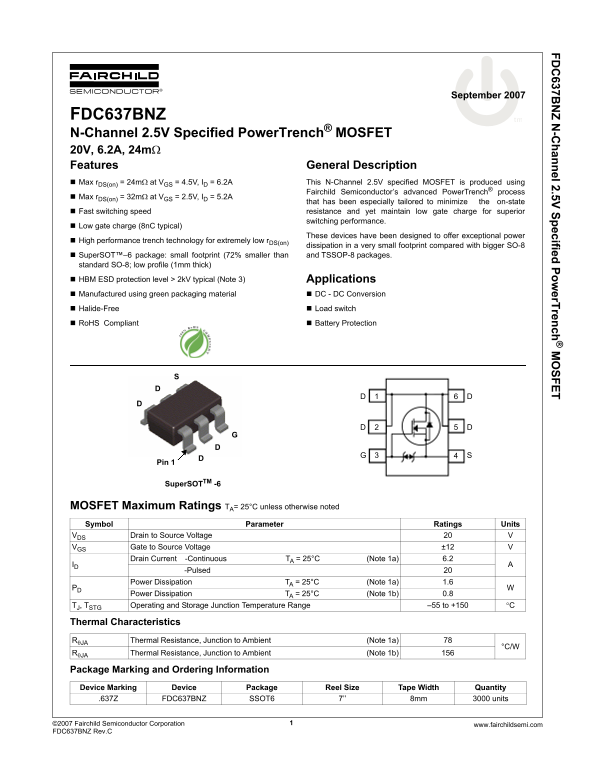
This advanced N-Channel PowerTrench MOSFET is designed for high-performance power management applications, including DC-DC converters, load switches, and battery protection circuits. Featuring extremely low $r_{DS(on)}$ and fast switching capabilities, it maintains superior efficiency in a compact SuperSOT™–6 package. Ideal for engineers seeking reliable, energy-efficient components that comply with ROHS standards.
Page 1 Text Content
FD 637B Z N -C hannel 2.5V Specified Pow er Trench SFET
September 2007
tm FDC637BNZ
N-Channel 2.5V Specified Power Trench® MOSFET 20V, 6.2A, 24mΩ Features General Description Max r DS(on) = 24mΩ at VGS = 4.5V, ID = 6.2A This N-Channel 2.5V specified MOSFET is produced using
Fairchild Semiconductor’s advanced Power Trench® process
Max r DS(on) = 32mΩ at VGS = 2.5V, ID = 5.2A
that has been especially tailored to minimize the on-state Fast switching speed resistance and yet maintain low gate charge for superior switching performance.
Low gate charge (8n C typical)
These devices have been designed to offer exceptional power
High performance trench technology for extremely low r DS(on)
dissipation in a very small footprint compared with bigger SO-8 Super SOT™–6 package: small footprint (72% smaller than and TSSOP-8 packages.
standard SO-8; low profile (1mm thick)
HBM ESD protection level > 2k V typical (Note 3) Applications Manufactured using green packaging material DC - DC Conversion Halide-Free Load switch Ro HS Compliant Battery Protection
Pin 1
Super SOTTM -6
MOSFET Maximum Ratings TA= 25°C unless otherwise noted Symbol Parameter Ratings Units VDS Drain to Source Voltage
VGS Gate to Source Voltage ±12 Drain Current -Continuous TA = 25°C (Note 1a) 6.2
-Pulsed Power Dissipation TA = 25°C (Note 1a) 1.6
Power Dissipation TA = 25°C (Note 1b) 0.8
TJ, TSTG Operating and Storage Junction Temperature Range –55 to +150 °C
Thermal Characteristics
RθJA Thermal Resistance, Junction to Ambient (Note 1a)
RθJA Thermal Resistance, Junction to Ambient (Note 1b)
Package Marking and Ordering Information Device Marking Device Package Reel Size Tape Width Quantity
.637Z FDC637BNZ SSOT6 7’’ 8mm 3000 units
©20 07 Fairchild Semiconductor Corporation www.fairchildsemi.com1 FD C637BNZ Rev.C
Page Summary Contents For Fairchild FDC637BNZ Specifications Manual
Manual Details
| Brand | Fairchild |
|---|---|
| Pages | 6 |
| File Size | 415.19 KB |
| Published | June 18, 2026 |
Enter the captcha to get the download link:

Frequently Asked Questions
What is the max continuous drain current?
6.2A at 25°C.
What package does this MOSFET use?
SuperSOT-6 package.
Can this MOSFET be used in life support devices?
No, not without express written approval.
What is the max on-resistance at 2.5V?
32mΩ at VGS=2.5V, ID=5.2A.