Fairchild Fan7842 Data Handbook
Summary
The FAN7842 is a high-voltage, monolithic gate driver IC designed for robust control of MOSFETs and IGBTs up to +200V. This manual provides detailed specifications on its key features, including floating channels supporting bootstrap operation, common-mode $\text{dv}/\text{dt}$ noise canceling, and TTL-compatible logic input. It is ideal for engineers designing demanding power electronics circuits such as half- and full-bridge converters, synchronous buck converters, and push-pull architectures requiring precise gate signal generation.
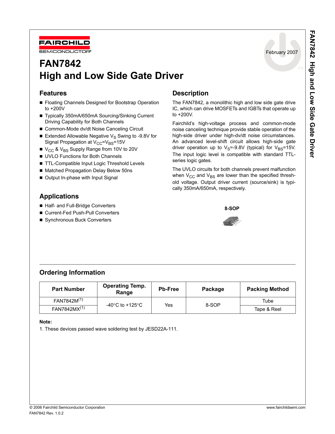
Page 1 Text Content
FA 7842 H igh and Low Side G ate D river
February 2007
FAN7842 High and Low Side Gate Driver Features Description Floating Channels Designed for Bootstrap Operation The FAN7842, a monolithic high and low side gate drive to +200V IC, which can drive MOSFETs and IGBTs that operate up
Typically 350m A/650m A Sourcing/Sinking Current to +200V.
Driving Capability for Both Channels
Fairchild’s high-voltage process and common-mode
Common-Mode dv/dt Noise Canceling Circuit noise canceling technique provide stable operation of the
Extended Allowable Negative VS Swing to -9.8V for high-side driver under high-dv/dt noise circumstances. Signal Propagation at VCC=VBS=15V An advanced level-shift circuit allows high-side gate driver operation up to VS=-9.8V (typical) for VBS=15V.
VCC & VBS Supply Range from 10V to 20V
The input logic level is compatible with standard TTL-
UVLO Functions for Both Channels
series logic gates.
TTL-Compatible Input Logic Threshold Levels
The UVLO circuits for both channels prevent malfunction
Matched Propagation Delay Below 50ns
when VCC and VBS are lower than the specified thresh-
Output In-phase with Input Signal
old voltage. Output driver current (source/sink) is typi- cally 350m A/650m A, respectively.
Applications Half- and Full-Bridge Converters
8-SOP
Current-Fed Push-Pull Converters Synchronous Buck Converters
Ordering Information
Operating Temp.
Part Number Pb-Free Package Packing Method
Range
FAN7842M(1) Tube
-40°C to +125°C Yes 8-SOP
FAN7842MX(1) Tape & Reel
Note: 1. These devices passed wave soldering test by JESD22A-111.
© 2006 Fairchild Semiconductor Corporation www.fairchildsemi.com FAN7842 Rev. 1.0.2
Page Summary Contents For Fairchild Fan7842 Data Handbook
Manual Details
| Brand | Fairchild |
|---|---|
| Pages | 13 |
| File Size | 365.11 KB |
| Published | July 06, 2026 |
Enter the captcha to get the download link:

Frequently Asked Questions
What voltage range is required for logic input (HIN/LIN)?
The logic input voltage (HIN, LIN) must be between -0.3V and +0.3V from V_IN.
What are the typical sourcing and sinking current capabilities?
The output driver current is typically 350mA for source and 650mA for sink.
What temperature range can this component operate in?
The ambient operating temperature range is -40°C to +125°C.
For what types of power conversion circuits is this driver suitable?
It is designed for applications such as Half- and Full-Bridge Converters, Current-Fed Push-Pull Converters, and Synchronous Buck Converters.