Fairchild FAN7383 Data Handbook
Summary
The FAN7383 is a high-voltage half-bridge gate-drive IC designed for driving MOSFETs and IGBTs up to 600V. It features programmable dead-time control, common-mode noise cancellation, and robust UVLO functions, making it ideal for SMPS, motor drives, and ballasts.
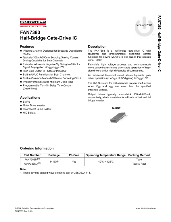
Page 1 Text Content
FA 7383 H alf-B ridge G ate-D rive IC
February 2007
FAN7383 Half-Bridge Gate-Drive IC Features Description Floating Channel Designed for Bootstrap Operation to The FAN7383 is a half-bridge gate-drive IC with +600V. shutdown and programmable dead-time control
Typically 350m A/650m A Sourcing/Sinking Current functions for driving MOSFETs and IGBTs that operate Driving Capability for Both Channels up to +600V.
Extended Allowable Negative VS Swing to -9.8V for Fairchild’s high voltage process and common-mode Signal Propagation at VDD=VBS=15V noise canceling technique give stable operation of high-
High-Side Output in Phase of IN Signal side drivers under high-dv/dt noise circumstances.
Built-in UVLO Functions for Both Channels An advanced level-shift circuit allows high-side gate Built-in Common-Mode dv/dt Noise Canceling Circuit driver operation up to VS= -9.8V (typical) for VBS=15V. Typically Internal 330ns Minimum Dead-Time
The UVLO circuits for both channels prevent malfunction
Programmable Turn-On Delay Time Control
when VDD and VBS are lower than the specified
(Dead-Time)
threshold voltage. Output drivers typically source/sink 350m A/650m A, Applications respectively, which is suitable for all kinds of half and full bridge inverter.
SMPS Motor Drive Inverter
14-SOP
Fluorescent Lamp Ballast HID Ballast
Ordering Information Part Number Package Pb-Free Operating Temperature Range Packing Method FAN7383M(1) Tube
14-SOP Yes -40°C ~ 125°C
FAN7383MX(1) Tape & Reel
Note: 1. These devices passed wave soldering test by JESD22A-111.
© 2006 Fairchild Semiconductor Corporation www.fairchildsemi.com FAN7383 Rev. 1.0.3
Page Summary Contents For Fairchild FAN7383 Data Handbook
Manual Details
| Brand | Fairchild |
|---|---|
| Pages | 16 |
| File Size | 1.23 MB |
| Published | June 16, 2026 |
Enter the captcha to get the download link:

Frequently Asked Questions
What is the maximum supply voltage for the high-side floating driver?
The high-side floating supply voltage (V_B) can be up to 625V, but the offset voltage (V_S) is rated for +600V operation.
What is the typical drive current capability?
It can typically source 350mA and sink 650mA for both high-side and low-side outputs.
What is the internal dead-time minimum?
It has a typical internal minimum dead-time of 330ns.
How is the dead-time programmed?
Dead-time is programmed using an external resistor connected to the DT pin.
What logic signal triggers a shutdown?
A low signal on the SD (shutdown) pin activates the shutdown function.