Fairchild Fan3122T Data Handbook
Summary
These high-speed, low-side gate drivers (FAN3121/FAN3122) are designed for efficiently switching N-channel MOSFETs in demanding power applications. They deliver high peak current pulses and feature advanced MillerDrive™ technology to ensure excellent performance across a wide operating temperature range. This manual provides comprehensive specifications, including pin configurations, thermal characterization data, and ordering guidelines necessary for seamless implementation. Ideal for engineers developing switch-mode power supplies, DC-to-DC converters, or motor control systems requiring robust MOSFET gate drive solutions.
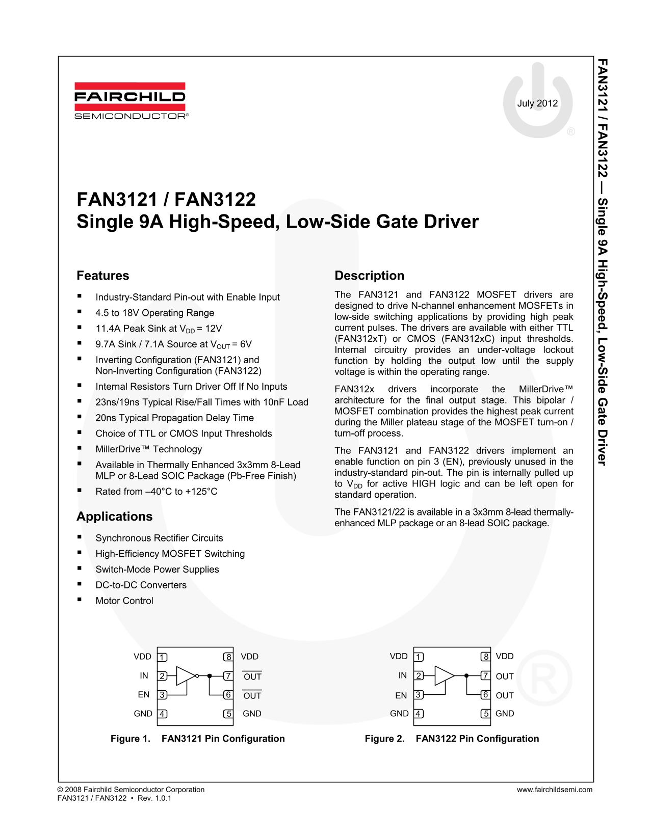
Page 1 Text Content
3121 / F 3122 — in le 9A ig -S eed , L -S id e G ate D river
July 2012
FAN3121 / FAN3122 Single 9A High-Speed, Low-Side Gate Driver
Features Description
Industry-Standard Pin-out with Enable Input The FAN3121 and FAN3122 MOSFET drivers are designed to drive N-channel enhancement MOSFETs in
4.5 to 18V Operating Range
low-side switching applications by providing high peak 11.4A Peak Sink at VDD = 12V current pulses. The drivers are available with either TTL (FAN312x T) or CMOS (FAN312x C) input thresholds.
9.7A Sink / 7.1A Source at VOUT = 6V
Internal circuitry provides an under-voltage lockout
Inverting Configuration (FAN3121) and function by holding the output low until the supply Non-Inverting Configuration (FAN3122) voltage is within the operating range. Internal Resistors Turn Driver Off If No Inputs
FAN312x drivers incorporate the Miller Drive™ 23ns/19ns Typical Rise/Fall Times with 10n F Load architecture for the final output stage. This bipolar / MOSFET combination provides the highest peak current
20ns Typical Propagation Delay Time
during the Miller plateau stage of the MOSFET turn-on / Choice of TTL or CMOS Input Thresholds turn-off process.
Miller Drive™ Technology The FAN3121 and FAN3122 drivers implement an
enable function on pin 3 (EN), previously unused in the
Available in Thermally Enhanced 3x3mm 8-Lead
industry-standard pin-out. The pin is internally pulled up
MLP or 8-Lead SOIC Package (Pb-Free Finish)
to VDD for active HIGH logic and can be left open for
Rated from –40°C to +125°C
standard operation. The FAN3121/22 is available in a 3x3mm 8-lead thermally-
Applications
enhanced MLP package or an 8-lead SOIC package.
Synchronous Rectifier Circuits High-Efficiency MOSFET Switching Switch-Mode Power Supplies DC-to-DC Converters Motor Control
VDD VDD VDD VDD
IN OUT IN OUT
EN OUT EN OUT
GND GND GND GND
Figure 1. FAN3121 Pin Configuration Figure 2. FAN3122 Pin Configuration
© 2008 Fairchild Semiconductor Corporation www.fairchildsemi.com FAN3121 / FAN3122 • Rev. 1.0.1
Page Summary Contents For Fairchild Fan3122T Data Handbook
Manual Details
| Brand | Fairchild |
|---|---|
| Pages | 23 |
| File Size | 1.59 MB |
| Published | July 07, 2026 |
Enter the captcha to get the download link:

Frequently Asked Questions
How is the gate driver enabled or inhibited?
The device uses pin EN; pulling this pin LOW will inhibit the driver function.
What is the primary difference between FAN3121 and FAN3122?
FAN3121 operates as an inverting configuration, while FAN3122 is designed for non-inverting operation.
What input logic thresholds are available?
Options include TTL or CMOS thresholds to match different system voltages and requirements.
How fast can these drivers switch mosfets?
They provide high speed characterized by 23ns/19ns typical rise/fall times with a 10nF load MOSFET combination.
What packages are available for PCB mounting?
The drivers are available in either an 8-Lead MLP (3x3mm) or an 8-lead SOIC package.