# A B C D E F G H I J K L M N O P Q R S T U V W X Y Z

Fairchild Fan3111C Data Handbook

Summary

The FAN3111 is a high-speed, single 1A low-side gate driver designed for robust MOSFET switching in diverse power applications. Featuring advanced input options—including dual CMOS inputs and external voltage referencing—it ensures reliable control across varying supply voltages (2V to 18V). This manual provides detailed technical specifications, operational guidelines, package details, and application guidance for engineers designing switch-mode power supplies, synchronous rectifiers, and motor control circuits.
📄 Preview PAGE OF 18

Page 1 Text Content

3111 — in le 1A ig -S eed , L -S id e G ate D river

July 2012

FAN3111 — Single 1A High-Speed, Low-Side Gate Driver Features Description

 1.4A Peak Sink / Source at VDD = 12V The FAN3111 1A gate driver is designed to drive an N- channel enhancement-mode MOSFET in low-side

 1.1A Sink / 0.9A Source at VOUT = 6V

switching applications.

 4.5 to 18V Operating Range

Two input options are offered: FAN3111C has dual  FAN3111C Compatible with FAN3100C Footprint CMOS inputs with thresholds referenced to VDD for use with PWM controllers and other input-signal sources that

 Two Input Configurations:

operate from the same supply voltage as the driver. For  Dual CMOS Inputs Allow Configuration as use with low-voltage controllers and other input-signal sources that operate from a lower supply voltage than

Non-Inverting or Inverting with Enable Function

the driver, that supply voltage may also be used as the

 Single Non-Inverting, Low-Voltage Input for

reference for the input thresholds of the FAN3111E.

Compatibility with Low-Voltage Controllers

This driver has a single, non-inverting, low-voltage input plus a DC input VXREF for an external reference voltage

 Small Footprint Facilitates Distributed Drivers for

in the range 2 to 5V.

Parallel Power Devices

 15ns Typical Delay Times The FAN3111 is available in a lead-free finish industry- standard 5-pin SOT23.

 9ns Typical Rise / 8ns Typical Fall times with 470p F Load  5-Pin SOT23 Package  Rated from –40°C to 125°C Ambient

Applications  Switch-Mode Power Supplies  Synchronous Rectifier Circuits  Pulse Transformer Driver  Logic to Power Buffer  Motor Control

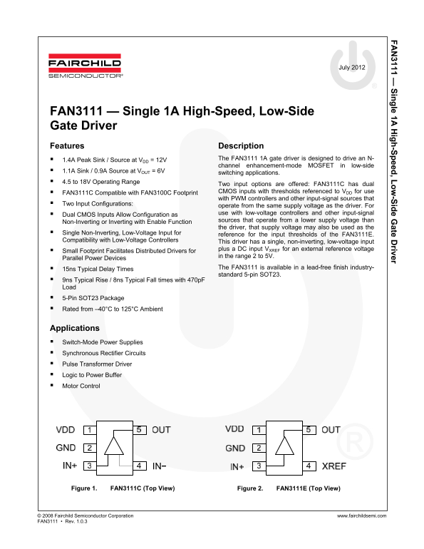
Figure 1. FAN3111C (Top View) Figure 2. FAN3111E (Top View)

© 2008 Fairchild Semiconductor Corporation www.fairchildsemi.com FAN3111 • Rev. 1.0.3

Page Summary Contents For Fairchild Fan3111C Data Handbook

Page 1 3111 — in le 1A ig -S eed , L -S id e G ate D river July 2012 FAN3111 — Single 1A High-Speed, Low-Side Gate Driver Features Description  1.4A Peak Sink / Source at VDD = 12V The FAN3111 1A gate drive...
Page 2 3111 — in le 1A ig -S eed , L -S id e G ate D river Ordering Information Input Quantity per Part Number Package Packing Method Threshold Reel FAN3111CSX CMOS 5-Pin SOT23 Tape & Reel 3,000 FAN3111E...
Page 3 3111 — in le 1A ig -S eed , L -S id e G ate D river Block Diagrams IN- GND Figure 3. FAN3111C Simplified Block Diagram IN+ OUT Figure 4. FAN3111E Simplified Block Diagram © 2008 Fairchild Semiconducto...
Page 4 3111 — in le 1A ig -S eed , L -S id e G ate D river Absolute Maximum Ratings Stresses exceeding the absolute maximum ratings may damage the device. The device may not function or be operable above the...
Page 5 3111 — in le 1A ig -S eed , L -S id e G ate D river Electrical Characteristics Unless otherwise noted, VDD = 12V, VXREF = 3.3V, TJ = -40°C to +125°C. Currents are defined as positive into the device a...
Page 6 3111 — in le 1A ig -S eed , L -S id e G ate D river Timing Diagrams Output 90% Output IN+ VINH IN - VINL t RISE t FALL t FALL t RISE Figure 5. Non-Inverting Waveforms Figure 6. Inverting Waveforms © 2...
Page 7 3111 — in le 1A ig -S eed , L -S id e G ate D river Typical Performance Characteristics Typical characteristics are provided at 25°C, VDD = 12V, and VXREF = 3.3V unless otherwise noted. (μ FAN3111E FA...
Page 8 3111 — in le 1A ig -S eed , L -S id e G ate D river Typical Performance Characteristics In re sh ld In re sh ld (V Typical characteristics are provided at 25°C, VDD = 12V, and VXREF = 3.3V unless othe...
Page 9 3111 — in le 1A ig -S eed , L -S id e G ate D river Typical Performance Characteristics ro ag at io el ay (n s) ro ag at io el ay (n s) In re sh ld (V Typical characteristics are provided at 25°C, VDD...
Page 10 3111 — in le 1A ig -S eed , L -S id e G ate D river Typical Performance Characteristics is im (n s) Typical characteristics are provided at 25°C, VDD = 12V, and VXREF = 3.3V unless otherwise noted. ro...
Page 11 3111 — in le 1A ig -S eed , L -S id e G ate D river Typical Performance Characteristics Typical characteristics are provided at 25°C, VDD = 12V, and VXREF = 3.3V unless otherwise noted. Figure 31. Qua...
Page 12 3111 — in le 1A ig -S eed , L -S id e G ate D river Applications Information The FAN3111 offers CMOS- or logic-level-compatible Figure 36 illustrates startup operation as VDD increases input threshold...
Page 13 3111 — in le 1A ig -S eed , L -S id e G ate D river The output-pin slew rate is determined by VDD voltage  Keep the driver as close to the load as possible to and the load on the output. It is not us...
Page 14 3111 — in le 1A ig -S eed , L -S id e G ate D river Truth Table of Logic Operation Thermal Guidelines The FAN3111 truth table indicates the operational states Gate drivers used to switch MOSFETs and I...
Page 15 3111 — in le 1A ig -S eed , L -S id e G ate D river Typical Application Diagrams Rectified AC Input Downstream Converters FAN3111 Logic PWM DD FAN3111 Figure 43. PFC Boost Circuit Utilizing Distribute...
Page 16 3111 — in le 1A ig -S eed , L -S id e G ate D river Table 2. Related Products Part Input Type Drive(10) Logic Package Number Threshold (Sink/Src) FAN3111C Single 1A +1.1A / -0.9A CMOS Single Channel o...
Page 17 3111 — in le 1A ig -S eed , L -S id e G ate D river Physical Dimensions TOP VIEW LAND PATTERN RECOMMENDATION SEE DETAIL A 1.45 MAX NOTES: UNLESS OTHEWISE SPECIFIED A) THIS PACKAGE CONFORMS TO JEDEC MO...
Page 18 3111 — in le 1A ig -S eed , L -S id e G ate D river © 2008 Fairchild Semiconductor Corporation www.fairchildsemi.com FAN3111 • Rev. 1.0.3 18

Manual Details

Brand Fairchild
Pages 18
File Size 1.09 MB
Published June 02, 2026
69 views

Enter the captcha to get the download link:

captcha

Frequently Asked Questions

What is the operating range for the FAN3111 gate driver?

The device operates in a 4.5 to 18V voltage range.

Which models are suitable when using external reference voltages (XREF)?

The FAN3111E model includes an XREF pin and is designed for external reference voltages between 2V and 5V.

What are the typical switching speeds of this driver?

It offers a typical delay time of 15ns, with rise/fall times of 9ns (rise) and 8ns (fall) when driving a 470pF load.

How does the FAN3111C enable its output using dual CMOS inputs?

The FAN3111C allows configuration as non-inverting, inverting, or single active input by connecting the IN+ and IN– pins to VDD or GND.