Fairchild DM7473 Data Handbook
Summary
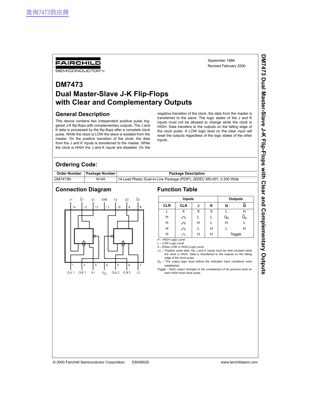
The DM7473 is a high-performance dual master-slave J-K Flip-Flop featuring clear inputs and complementary outputs. This robust integrated circuit processes sequential logic data based on precise clock pulse transitions, making it ideal for complex digital timing applications. The comprehensive technical manual provides engineers with detailed electrical characteristics, absolute maximum ratings, switching parameters, and operational guidelines needed to reliably implement this foundational component in their electronic designs.
Page 1 Text Content
7473 D al M aster-S lave J-K lip -F lo s w ith lear an lem en tary O tp ts
September 1986 Revised February 2000
DM7473 Dual Master-Slave J-K Flip-Flops with Clear and Complementary Outputs
negative transition of the clock, the data from the master is
General Description
transferred to the slave. The logic states of the J and K
This device contains two independent positive pulse trig-
inputs must not be allowed to change while the clock is
gered J-K flip-flops with complementary outputs. The J and
HIGH. Data transfers to the outputs on the falling edge of
K data is processed by the flip-flops after a complete clock
the clock pulse. A LOW logic level on the clear input will
pulse. While the clock is LOW the slave is isolated from the
reset the outputs regardless of the logic states of the other
master. On the positive transition of the clock, the data
inputs.
from the J and K inputs is transferred to the master. While the clock is HIGH the J and K inputs are disabled. On the
Ordering Code: Order Number Package Number Package Description DM7473N N14A 14-Lead Plastic Dual-In-Line Package (PDIP), JEDEC MS-001, 0.300 Wide
Connection Diagram Function Table
Inputs Outputs
CLR CLK
Toggle
H = HIGH Logic Level L = LOW Logic Level X = Either LOW or HIGH Logic Level = Positive pulse data. the J and K inputs must be held constant while the clock is HIGH. Data is transferred to the outputs on the falling edge of the clock pulse. Q0 = The output logic level before the indicated input conditions were established. Toggle = Each output changes to the complement of its previous level on each HIGH level clock pulse.
© 2000 Fairchild Semiconductor Corporation DS006525 www.fairchildsemi.com
Page Summary Contents For Fairchild DM7473 Data Handbook
Manual Details
| Brand | Fairchild |
|---|---|
| Pages | 3 |
| File Size | 40.02 KB |
| Published | July 06, 2026 |
Enter the captcha to get the download link:

Frequently Asked Questions
What is the recommended operating temperature range?
The free air operating temperature range for recommended operation is 0°C to +70°C.
How does data transfer occur on this flip-flop?
Data transfers to the output on the falling edge of the clock pulse, and J/K inputs must be held constant while the clock is HIGH.
What happens if I activate the Clear input?
A LOW logic level on the clear input will immediately set the outputs to a known state regardless of data inputs or internal states.
What is the maximum usable clock frequency?
The maximum specified clock frequency (at 5V and 25°C) for this device is 15 MHz.