# A B C D E F G H I J K L M N O P Q R S T U V W X Y Z

Fairchild Design Guidelines for Offline Flyback Converters using FPS

Summary

Accelerate your SMPS design process with this professional application note on off-line flyback converters. This comprehensive guide is essential for engineers who need to build reliable Switched Mode Power Supplies (SMPS). It details a practical, step-by-step procedure for designing and selecting optimal components—including transformers, capacitors, and MOSFETs—to ensure efficient and stable converters. Use these proven guidelines to minimize design iterations and successfully integrate high-performance flyback converter solutions.
📄 Preview PAGE OF 20

Page 1 Text Content

www.fairchildsemi.com

Application Note AN4137 Design Guidelines for Off-line Flyback Converters Using Fairchild Power Switch (FPS)

Abstract The step-by-step design procedure described in this paper helps engineers to design SMPS easily. In order to make the

This paper presents practical design guidelines for off-line

design process more efficient, a software design tool, FPS

flyback converters employing FPS (Fairchild Power

design assistant that contains all the equations described in

Switch). Switched mode power supply (SMPS) design is

this paper is also provided. The design procedure is verified

inherently a time consuming job requiring many trade-offs

through experimental prototype converter.

and iterations with a large number of design variables.

DR(n) LP(n)

Bridge rectifier

VDC Rsn

diode Csn Vsn Np

NS(n)

VO(n)CP(n)

CO(n)

FPS DR1 LP1

Drain

CO1 CP1 VO1

AC line

FB Vcc

Da Ra

Rbias

Ca H11A817A

Na R1

RF CF

KA431

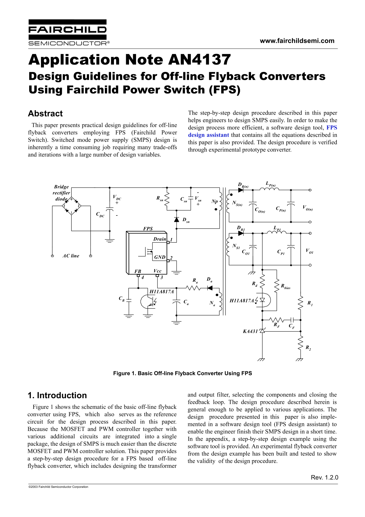
Figure 1. Basic Off-line Flyback Converter Using FPS

1. Introduction and output filter, selecting the components and closing the feedback loop. The design procedure described herein is

Figure 1 shows the schematic of the basic off-line flyback

general enough to be applied to various applications. The

converter using FPS, which also serves as the reference

design procedure presented in this paper is also imple-

circuit for the design process described in this paper.

mented in a software design tool (FPS design assistant) to

Because the MOSFET and PWM controller together with

enable the engineer finish their SMPS design in a short time.

various additional circuits are integrated into a single

In the appendix, a step-by-step design example using the

package, the design of SMPS is much easier than the discrete

software tool is provided. An experimental flyback converter

MOSFET and PWM controller solution. This paper provides

from the design example has been built and tested to show

a step-by-step design procedure for a FPS based off-line

the validity of the design procedure.

flyback converter, which includes designing the transformer

Rev. 1.2.0

©2003 Fairchild Semiconductor Corporation

Page Summary Contents For Fairchild Design Guidelines for Offline Flyback Converters using FPS

Page 1 www.fairchildsemi.com Application Note AN4137 Design Guidelines for Off-line Flyback Converters Using Fairchild Power Switch (FPS) Abstract The step-by-step design procedure described in this paper he...
Page 2 AN4137 APPLICATION NOTE 2. Step-by-step Design Procedure In this section, a design procedure is presented using the schematic of figure 1 as a reference. In general, most FPS devices have the same pin...
Page 3 APPLICATION NOTE AN4137 In the case of a CCM flyback converter, the design process is straight forward since the input-to-output voltage gain depends only on the duty cycle. Meanwhile, the input-to-ou...
Page 4 AN4137 APPLICATION NOTE nom would be (Dmax) should be determined so that Vds 65~70% of the MOSFET voltage rating considering the volt- 1– CCM age spike caused by the leakage inductance. In the case of...
Page 5 APPLICATION NOTE AN4137 Fl ux en sit (m T) With the chosen core, the minimum number of turns for the transformer primary side to avoid the core saturation is given Output EI core EE core EPC core EER ...
Page 6 AN4137 APPLICATION NOTE severe eddy current losses as well as to make winding easier. For high current output, it is better to use parallel windings with multiple strands of thinner wire to minimize s...
Page 7 APPLICATION NOTE AN4137 (10) STEP-10 : Determine the output capacitor considering the voltage and current ripple. Schottky Barrier Diode The ripple current of the n-th output capacitor (Co(n)) is Prod...
Page 8 AN4137 APPLICATION NOTE From equation (28), the maximum voltage stress on the inter- nal MOSFET is given by Vsn( )2 peak( Psn fs Ll K Ids (26) Rsn Vsn VRO– max max Vds VDC Vsn2+= (31) peak is specifie...
Page 9 APPLICATION NOTE AN4137 RL D–( )2 (12) STEP-12 : Design the feed back loop. D+( wz , wrz and wp Rc1Co1 RLCo1 Since most FPS devices employ current mode control as DLm Ns1 Np⁄( )2 shown in figure 12, t...
Page 10 AN4137 APPLICATION NOTE When the input voltage and the load current vary over a wide range, it is not easy to determine the worst case for the feed- v FB wi wzc⁄+ back loop design. The gain together w...
Page 11 APPLICATION NOTE AN4137 ing the startup. While, too large a capacitor may increase the When determining the feedback circuit component, there are startup time. some restrictions as follows. (b) Vcc re...
Page 12 AN4137 APPLICATION NOTE - Summary of symbols - Aw : Winding window area of the core in mm2 Ae : Cross sectional area of the core in mm2 Bsat : Saturation flux density in tesla. Co(n) : Output capacito...
Page 13 APPLICATION NOTE AN4137 Appendix : Design example using FPS Design Assistant Output Ripple Device Application Output voltage (Max Current)Input voltage Power spec 85V-265VAC47WFSDM07652RSet-top Box 12...
Page 14 AN4137 APPLICATION NOTE 5. Choose the proper FPS considering the input power and current limit Typical current limit of FPS (Iover) 2.50 Minimum Iover considering tolerance of 12% 2.20 2.01 ->O.K. ...
Page 15 APPLICATION NOTE AN4137 9. Choose the rectifier diode in the secondary side VD(n) ID(n) Vcc diode 0.10 1st output diode 3.50 2nd output diode 3.67 3rd output diode 2.75 4th output diode 0.95 5th outpu...
Page 16 AN4137 APPLICATION NOTE re in 12. Design Feedback control loop Control-to-output DC gain = Control-to-output zero (wz) = rad/s => fz= Hz Control-to-output RHP zero (wrz)= rad/s => frz= 110,631 H...
Page 17 APPLICATION NOTE AN4137 Design Summary For the FPS, FSDM07652R is chosen. This device has a fixed switching frequency of 66k Hz. Startup and soft-start circuits are implemented inside the device. To l...
Page 18 AN4137 APPLICATION NOTE Experimental Verification In order to show the validity of the design procedure pre- sented in this paper, the converter of the design example has been built and tested. All th...
Page 19 APPLICATION NOTE AN4137 Efficiency 0.81 0.80 0.79 0.78 0.77 0.76 0.75 0.74 0.73 0.72 Input voltage (Vac) Figure 22. Measured efficiency Figure 21. Current and voltage waveforms of the first output (3....
Page 20 AN4137 APPLICATION NOTE by Hang-Seok Choi / Ph. D FPS Application Group / Fairchild Semiconductor Phone : +82-32-680-1383 Facsimile : +82-32-680-1317 E-mail : [email protected] DISCLAIMER FAI...

Manual Details

Brand Fairchild
Pages 20
File Size 399.90 KB
Published July 22, 2026
0 views

Enter the captcha to get the download link:

captcha

Frequently Asked Questions

How do I generally start the SMPS design procedure?

The process begins by defining the system specifications, followed by determining the DC link capacitor and transformer parameters.

What is the recommended DC link capacitor value?

Use 2-3uF per watt for universal input range or 1uF per watt for European input range.

Is specialized software available to simplify the design process?

Yes, the FPS flyback converters utilize a dedicated software tool (FPS design assistant) to make SMPS design much easier and faster.

What is the policy regarding life support applications?

Fairchild products are not authorized for use as critical components in life support devices or systems without express written approval.