# A B C D E F G H I J K L M N O P Q R S T U V W X Y Z

Fairchild AN-6026 Specifications Manual

Summary

Designed for professionals building high-efficiency power supplies, this manual details the implementation of an Active Power Factor Correction (PFC) circuit using FAN7529 boost controllers. The guide provides comprehensive technical knowledge on both current and voltage modes of PFC operation. It meticulously covers the underlying circuitry, including detailed descriptions of critical internal blocks like the Zero Current Detector and Error Amplifier. Use this resource to understand how to design robust, optimal power factor conversion systems for demanding electrical applications.
📄 Preview PAGE OF 23

Page 1 Text Content

www.fairchildsemi.com

Application Note AN-6026 Design of Power Factor Correction Circuit Using FAN7529

1. Introduction FAN7527B; however, the sensing network can cause addi- tional power loss. In the voltage mode, the switch turn-on is

The FAN7529 is an active power factor correction (PFC)

the same as that of the current mode, but the switch turn-off

controller for the boost PFC application that operates in the

is determined by an internal ramp signal. The ramp signal is

critical conduction mode (CRM). The critical conduction

compared with an error amplifier output and the switch turn-

mode boost power factor converter operates at the boundary

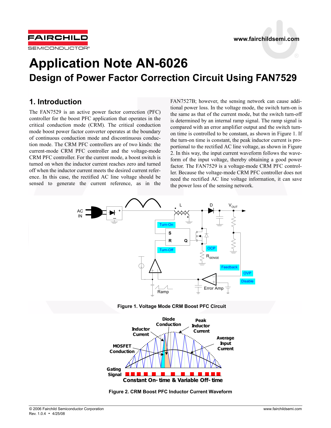
on time is controlled to be constant, as shown in Figure 1. If

of continuous conduction mode and discontinuous conduc-

the turn-on time is constant, the peak inductor current is pro-

tion mode. The CRM PFC controllers are of two kinds: the

portional to the rectified AC line voltage, as shown in Figure

current-mode CRM PFC controller and the voltage-mode

2. In this way, the input current waveform follows the wave-

CRM PFC controller. For the current mode, a boost switch is

form of the input voltage, thereby obtaining a good power

turned on when the inductor current reaches zero and turned

factor. The FAN7529 is a voltage-mode CRM PFC control-

off when the inductor current meets the desired current refer-

ler. Because the voltage-mode CRM PFC controller does not

ence. In this case, the rectified AC line voltage should be

need the rectified AC line voltage information, it can save

sensed to generate the current reference, as in the

the power loss of the sensing network.

AC IN

Turn- ur On

Turn- Off

RSENSE

Feedback

Disable

Error Amp

Figure 1. Voltage Mode CRM Boost PFC Circuit

Diode

Conduction

Inductor Current Inductor

Current

Average Input

MOSFET

Current

Conduction

Gating Signal Constant On- time & Variable Off- time

Figure 2. CRM Boost PFC Inductor Current Waveform

© 2006 Fairchild Semiconductor Corporation www.fairchildsemi.com Rev. 1.0.4 • 4/25/08

Page Summary Contents For Fairchild AN-6026 Specifications Manual

Page 1 www.fairchildsemi.com Application Note AN-6026 Design of Power Factor Correction Circuit Using FAN7529 1. Introduction FAN7527B; however, the sensing network can cause addi- tional power loss. In the ...
Page 2 AN6026 APPLICATION NOTE Block Diagram VCC Vref UVLO VCC Internal Bias 12V 8.5V Disable OUTDrive Output 150μs 13V Timer Zero Current OVP Detector 2.675V 2.5V Disable Current Protection 0.8V Comparator ...
Page 3 AN6026 APPLICATION NOTE 2. Device Block Description the junction capacitor of the MOSFET resonates with the boost inductor and the auxiliary winding voltage decreases 2.1 Error Amplifier Block resonan...
Page 4 AN6026 APPLICATION NOTE Ideally, the switch must be turned on when the inductor cur- rent reaches zero; but because of the structure of the ZCD Off Signal 1V Offset block and Rzcd delay, it is turned ...
Page 5 AN6026 APPLICATION NOTE 3.Circuit Components Design 3.1 Power Stage Design in peak in peak 1) Boost Inductor Design +⎜ ⎟⎜ sw (min) (max) ⎟−⎝ The boost inductor value is determined by the output power ...
Page 6 AN6026 APPLICATION NOTE leading current, which causes phase difference between the 4) Output Capacitor Design line current and the line voltage. The phase difference The output capacitor is selected b...
Page 7 AN6026 APPLICATION NOTE The switching frequency is the average value during a line period. The total MOSFET loss can be calculated by Equa- tion 19 and a MOSFET can be selected considering the PFC OUT...
Page 8 AN6026 APPLICATION NOTE imize the zero crossing distortion, COSS must be minimized VOUT and a larger inductor should be used. There is a limitation in minimizing COSS and using a large inductor becaus...
Page 9 AN6026 APPLICATION NOTE 3) Start-up Circuit Design To start up the FAN7529, the start-up current must be sup- plied through a start-up resistor. The resistor value is calcu- Output lated by Equations ...
Page 10 AN6026 APPLICATION NOTE 4. Design Example ZCD pin and the ground to increase the delay time for the MOSFET minimum voltage turn-on. A 100W converter is used here to illustrate the design proce- dure u...
Page 11 AN6026 APPLICATION NOTE T1 PFC OUTPUT BD C5 ZD1 C11 R6 D1 LF1 FAN7529 IN AC INPUT Figure 22. Application Circuit Schematic © 2006 Fairchild Semiconductor Corporation www.fairchildsemi.com Rev. 1.0.4 •...
Page 12 AN6026 APPLICATION NOTE Table 1. 100W Demo Board Part List (400µH, Wide Input Range Application) PART# VALUE NOTE PART# VALUE NOTE Fuse Capacitor F1 250V/3A C1 150n F/275VAC Box Capacitor TNR C2 470n ...
Page 13 AN6026 APPLICATION NOTE Table 3. 100W Demo Board Part List (600µH, Wide Input Range Application) PART# VALUE NOTE PART# VALUE NOTE Fuse Capacitor F1 250V/3A C1 150n F/275VAC Box Capacitor TNR C2 470n ...
Page 14 AN6026 APPLICATION NOTE Table 5. 32W Wide Input Range Application Part List PART# VALUE NOTE PART# VALUE NOTE Fuse Capacitor F1 250V/1A C1 47n F/275VAC Box Capacitor TNR C2 220n F/275VAC Box Capacitor...
Page 15 AN6026 APPLICATION NOTE Table 7. 32W 220VAC Input Application Part List PART# VALUE NOTE PART# VALUE NOTE Fuse Capacitor F1 250V/1A C1 47n F/275VAC Box Capacitor TNR C2 267n F/275VAC Box Capacitor V1 ...
Page 16 AN6026 APPLICATION NOTE Table 9. 64W Wide Input Range Application Part List PART# VALUE NOTE PART# VALUE NOTE Fuse Capacitor F1 250V/2A C1 47n F/275VAC Box Capacitor TNR C2 330n F/275VAC Box Capacitor...
Page 17 AN6026 APPLICATION NOTE Table 11. 64W 220VAC Input Application Part List PART# VALUE NOTE PART# VALUE NOTE Fuse Capacitor F1 250V/2A C1 47n F/275VAC Box Capacitor TNR C2 330n F/275VAC Box Capacitor V1...
Page 18 AN6026 APPLICATION NOTE Table 13. 100W 220VAC Input Application Part List PART# VALUE NOTE PART# VALUE NOTE Fuse Capacitor F1 250V/3A C1 150n F/275VAC Box Capacitor TNR C2 470n F/275VAC Box Capacitor ...
Page 19 AN6026 APPLICATION NOTE Table 15. 150W Wide Input Range Application Part List PART# VALUE NOTE PART# VALUE NOTE Fuse Capacitor F1 250V/3A C1 150n F/275VAC Box Capacitor TNR C2 470n F/275VAC Box Capaci...
Page 20 AN6026 APPLICATION NOTE Table 17. 150W 220VAC Input Application Part List PART# VALUE NOTE PART# VALUE NOTE Fuse Capacitor F1 250V/3A C1 150n F/275VAC Box Capacitor TNR C2 470n F/275VAC Box Capacitor ...
Page 21 AN6026 APPLICATION NOTE Table 19. 200W Wide Input Range Application Part List PART# VALUE NOTE PART# VALUE NOTE Fuse Capacitor F1 250V/5A C1 470n F/275VAC Box Capacitor TNR C2 470n F/275VAC Box Capaci...
Page 22 AN6026 APPLICATION NOTE Nomenclature Ccomp: compensation capacitance Naux: auxiliary winding turn number CIN: input capacitance NP: boost inductor turn number COUT: output capacitance Pin: input power...
Page 23 AN6026 APPLICATION NOTE DISCLAIMER FAIRCHILD SEMICONDUCTOR RESERVES THE RIGHT TO MAKE CHANGES WITHOUT FURTHER NOTICE TO ANY PRODUCTS HEREIN TO IMPROVE RELIABILITY, FUNCTION, OR DESIGN. FAIRCHILD DOES ...

Manual Details

Brand Fairchild
Pages 23
File Size 346.51 KB
Published July 06, 2026
4 views

Enter the captcha to get the download link:

captcha

Frequently Asked Questions

How does the Zero Current Detector (ZCD) function?

The ZCD generates the MOSFET turn-on signal when the boost inductor current reaches zero, utilizing an auxiliary winding for detection.

What are the thresholds for Over-Voltage Protection (OVP)?

OVP shuts down the output drive block if the input voltage (V_IN) is higher than 2.675V, allowing a 0.175V hysteresis.

How can I externally disable the IC?

An external, small-signal 6.5V to 1.5V MOSFET can be used to manually disable the IC and reduce power consumption.

Can the FAN7529 be used in life support systems?

No; Fairchild’s products are not authorized for use as critical components in life support devices or systems without express written approval.