FAIRCHILD 74VCX16244 Data Handbook
Summary
The 74VCX16244 is a high-speed, low-voltage 16-bit buffer and line driver featuring sixteen non-inverting buffers with 3-STATE outputs and 3.6V tolerant inputs/outputs. Engineered for applications requiring robust signal integrity at voltages between 1.2V and 3.6V. This manual provides comprehensive details, including electrical specifications, pin descriptions (FBGA/TSSOP), and detailed operational data necessary for integrating the device into complex digital bus systems. It is ideal for electronic designers building low-power or sensitive communication circuits.
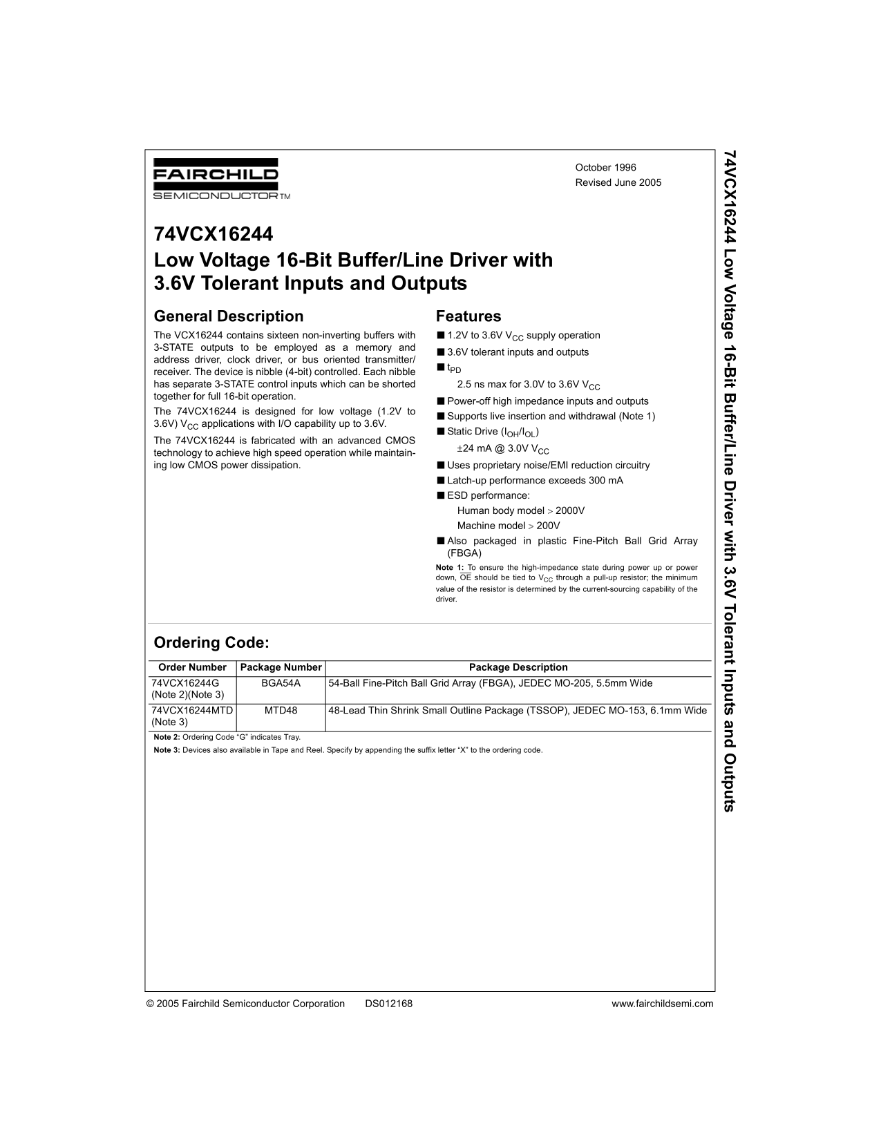
Page 1 Text Content
74V 16244 L Vo ltag e 16-B it B ffer/L in e D river w ith 3.6V To leran t In ts an tp ts
October 1996 Revised June 2005
74VCX16244 Low Voltage 16-Bit Buffer/Line Driver with 3.6V Tolerant Inputs and Outputs General Description Features The VCX16244 contains sixteen non-inverting buffers with ■1.2V to 3.6V VCC supply operation 3-STATE outputs to be employed as a memory and
■3.6V tolerant inputs and outputs
address driver, clock driver, or bus oriented transmitter/
receiver. The device is nibble (4-bit) controlled. Each nibble has separate 3-STATE control inputs which can be shorted 2.5 ns max for 3.0V to 3.6V VCC together for full 16-bit operation.
■Power-off high impedance inputs and outputs
The 74VCX16244 is designed for low voltage (1.2V to
■Supports live insertion and withdrawal (Note 1)
3.6V) VCC applications with I/O capability up to 3.6V.
■Static Drive (IOH/IOL)
The 74VCX16244 is fabricated with an advanced CMOS
r24 m A @ 3.0V VCC
technology to achieve high speed operation while maintain- ing low CMOS power dissipation. ■Uses proprietary noise/EMI reduction circuitry
■Latch-up performance exceeds 300 m A ■ESD performance: Human body model ! 2000V Machine model ! 200V ■Also packaged in plastic Fine-Pitch Ball Grid Array (FBGA) Note 1: To ensure the high-impedance state during power up or power down, OE should be tied to VCC through a pull-up resistor; the minimum value of the resistor is determined by the current-sourcing capability of the driver.
Ordering Code: Order Number Package Number Package Description 74VCX16244G BGA54A 54-Ball Fine-Pitch Ball Grid Array (FBGA), JEDEC MO-205, 5.5mm Wide (Note 2)(Note 3) 74VCX16244MTD MTD48 48-Lead Thin Shrink Small Outline Package (TSSOP), JEDEC MO-153, 6.1mm Wide (Note 3) Note 2: Ordering Code “G” indicates Tray. Note 3: Devices also available in Tape and Reel. Specify by appending the suffix letter “X” to the ordering code.
© 2005 Fairchild Semiconductor Corporation DS012168 www.fairchildsemi.com
Page Summary Contents For FAIRCHILD 74VCX16244 Data Handbook
Manual Details
| Brand | Fairchild |
|---|---|
| Pages | 10 |
| File Size | 117.70 KB |
| Published | June 22, 2026 |
Enter the captcha to get the download link:

Frequently Asked Questions
What precautions are needed when connecting the Output Enable (OE) input?
To ensure high-impedance state during power up or down, OE must be tied to VCC through a pull-up resistor.
What voltage range is the 74VCX16244 designed for?
It supports low voltages operating from 1.2V up to recommendable maximum of 3.6V.
How do I achieve full 16-bit operation with this device?
Full 16-bit operation is achieved by shorting the four separate nibble control inputs together.
Are these components suitable for critical life support applications?
No, they are not authorized for use as critical components in life support devices without written approval.