Fairchild 74VCX162240 Data Handbook
Summary
The 74VCX162240 is a robust, low-voltage 16-bit inverting buffer and line driver engineered for demanding digital applications requiring high signal integrity. Featuring 3.6V tolerant inputs/outputs and integrated 26Ω series resistors, this device minimizes noise when used as memory address or clock bus transceivers across the 1.65V to 3.6V range. This documentation provides critical technical specifications, detailed electrical characteristics, operating conditions, and functional descriptions necessary for hardware engineers designing reliable low-power CMOS systems.
Page 1 Text Content
查询74VCX162240供应商
74V 162240 L Vo ltag e 16-B it In vertin ffer/L in e D river w ith 3.6V To leran t In ts an tp ts an 26Ω eries R esisto rs in tp ts
January 1998 Revised April 1999
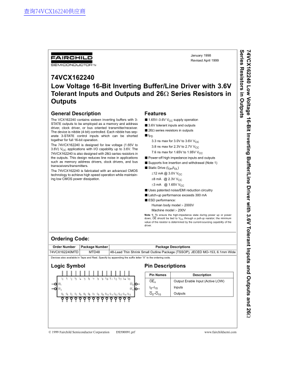
74VCX162240 Low Voltage 16-Bit Inverting Buffer/Line Driver with 3.6V Tolerant Inputs and Outputs and 26Ω Series Resistors in Outputs General Description Features The VCX162240 contains sixteen inverting buffers with 3- 1.65V–3.6V VCC supply operation STATE outputs to be employed as a memory and address
3.6V tolerant inputs and outputs
driver, clock driver, or bus oriented transmitter/receiver.
26Ω series resistors in outputs
The device is nibble (4-bit) controlled. Each nibble has sep-
arate 3-STATE control inputs which can be shorted t PD
together for full 16-bit operation.
3.3 ns max for 3.0V to 3.6V VCC
The 74VCX162240 is designed for low voltage (1.65V to
3.8 ns max for 2.3V to 2.7V VCC
3.6V) VCC applications with I/O capability up to 3.6V. The
7.6 ns max for 1.65V to 1.95V VCC
74VCX162240 is also designed with 26Ω series resistors in the outputs. This design reduces line noise in applications Power-off high impedance inputs and outputs such as memory address drivers, clock drivers, and bus
Supports live insertion and withdrawal (Note 1)
transceivers/transmitters.
Static Drive (IOH/IOL)
The 74VCX162240 is fabricated with an advanced CMOS
±12 m A @ 3.0V VCC
technology to achieve high speed operation while maintain- ing low CMOS power dissipation. ±8 m A @ 2.3V VCC
±3 m A @ 1.65V VCC Uses patented noise/EMI reduction circuitry Latch-up performance exceeds 300 m A ESD performance: Human body model > 2000V Machine model > 200V Note 1: To ensure the high-impedance state during power up or power down, OE should be tied to VCC through a pull-up resistor; the minimum value of the resistor is determined by the current-sourcing capability of the driver.
Ordering Code: Order Number Package Number Package Descriptions 74VCX162240MTD MTD48 48-Lead Thin Shrink Small Outline Package (TSSOP), JECED MO-153, 6.1mm Wide Devices also available in Tape and Reel. Specify by appending the suffix letter “X” to the ordering code.
Logic Symbol Pin Descriptions
Pin Names Description
OEn Output Enable Input (Active LOW)
I0–I15 Inputs
O0–O15 Outputs
© 1999 Fairchild Semiconductor Corporation DS500091.prf www.fairchildsemi.com
Page Summary Contents For Fairchild 74VCX162240 Data Handbook
Manual Details
| Brand | Fairchild |
|---|---|
| Pages | 8 |
| File Size | 59.59 KB |
| Published | June 02, 2026 |
Enter the captcha to get the download link:
