Fairchild 74LCX00 Data Handbook
Summary
The 74LCX00 is a quad 2-input NAND gate utilizing advanced CMOS technology, engineered for mixed-voltage systems requiring high reliability. Its standout feature is 5V tolerance up to 7V inputs, allowing seamless interfacing between standard 3V logic circuits and higher voltage infrastructure. This guide provides comprehensive technical details for system designers and electronics engineers, covering stringent electrical characteristics, absolute maximum ratings, recommended operating conditions across temperature variations, and multiple leadless package options (DQFN, SOIC, etc.).
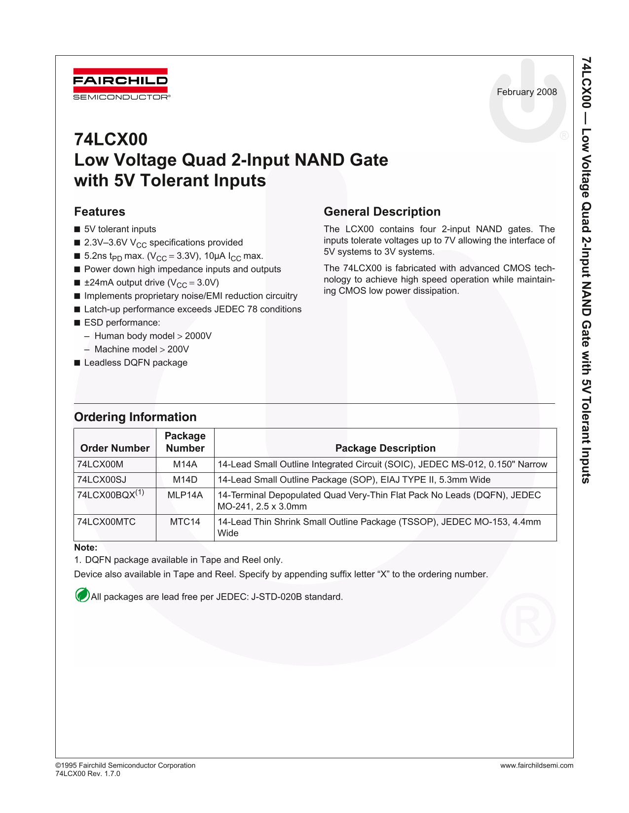
Page 1 Text Content
74L 00 — Vo ltag e Q ad 2-In t N ate w ith 5V To leran t In ts
February 2008
74LCX00 Low Voltage Quad 2-Input NAND Gate with 5V Tolerant Inputs Features General Description 5V tolerant inputs The LCX00 contains four 2-input NAND gates. The
2.3V–3.6V VCC specifications provided inputs tolerate voltages up to 7V allowing the interface of 5V systems to 3V systems.
5.2ns t PD max. (VCC = 3.3V), 10µA ICC max.
Power down high impedance inputs and outputs The 74LCX00 is fabricated with advanced CMOS tech- nology to achieve high speed operation while maintain-
±24m A output drive (VCC = 3.0V)
ing CMOS low power dissipation.
Implements proprietary noise/EMI reduction circuitry Latch-up performance exceeds JEDEC 78 conditions ESD performance: – Human body model > 2000V – Machine model > 200V Leadless DQFN package
Ordering Information
Package
Order Number Number Package Description 74LCX00M M14A 14-Lead Small Outline Integrated Circuit (SOIC), JEDEC MS-012, 0.150" Narrow 74LCX00SJ M14D 14-Lead Small Outline Package (SOP), EIAJ TYPE II, 5.3mm Wide
74LCX00BQX(1) MLP14A 14-Terminal Depopulated Quad Very-Thin Flat Pack No Leads (DQFN), JEDEC
MO-241, 2.5 x 3.0mm
74LCX00MTC MTC14 14-Lead Thin Shrink Small Outline Package (TSSOP), JEDEC MO-153, 4.4mm
Note: 1. DQFN package available in Tape and Reel only. Device also available in Tape and Reel. Specify by appending suffix letter “X” to the ordering number.
All packages are lead free per JEDEC: J-STD-020B standard.
©1 995 Fairchild Semiconductor Corporation www.fairchildsemi.com 74L CX00 Rev. 1.7.0
Page Summary Contents For Fairchild 74LCX00 Data Handbook
Manual Details
| Brand | Fairchild |
|---|---|
| Pages | 13 |
| File Size | 771.28 KB |
| Published | July 16, 2026 |
Enter the captcha to get the download link:

Frequently Asked Questions
What is the primary function of the 74LCX00?
It is a Low Voltage Quad 2-Input NAND Gate designed to handle inputs up to 5V, suitable for interfacing 2.3V–3.6V CC systems with 3V systems.
Are there limits on using this device in life support equipment?
No, Fairchild's products are not authorized for use as critical components in life support devices or systems without express written approval.
What are the available packaging options and how do I order them?
Available packages include SOIC, SOP, MLP (DQFN), and TSSOP. For DQFN, remember to specify a suffix 'X' when ordering.
What is the recommended operating temperature range for this device?
The recommended free-air operating temperature range is from –40°C to +85°C.