Fairchild 74LC244 Data Handbook
Summary
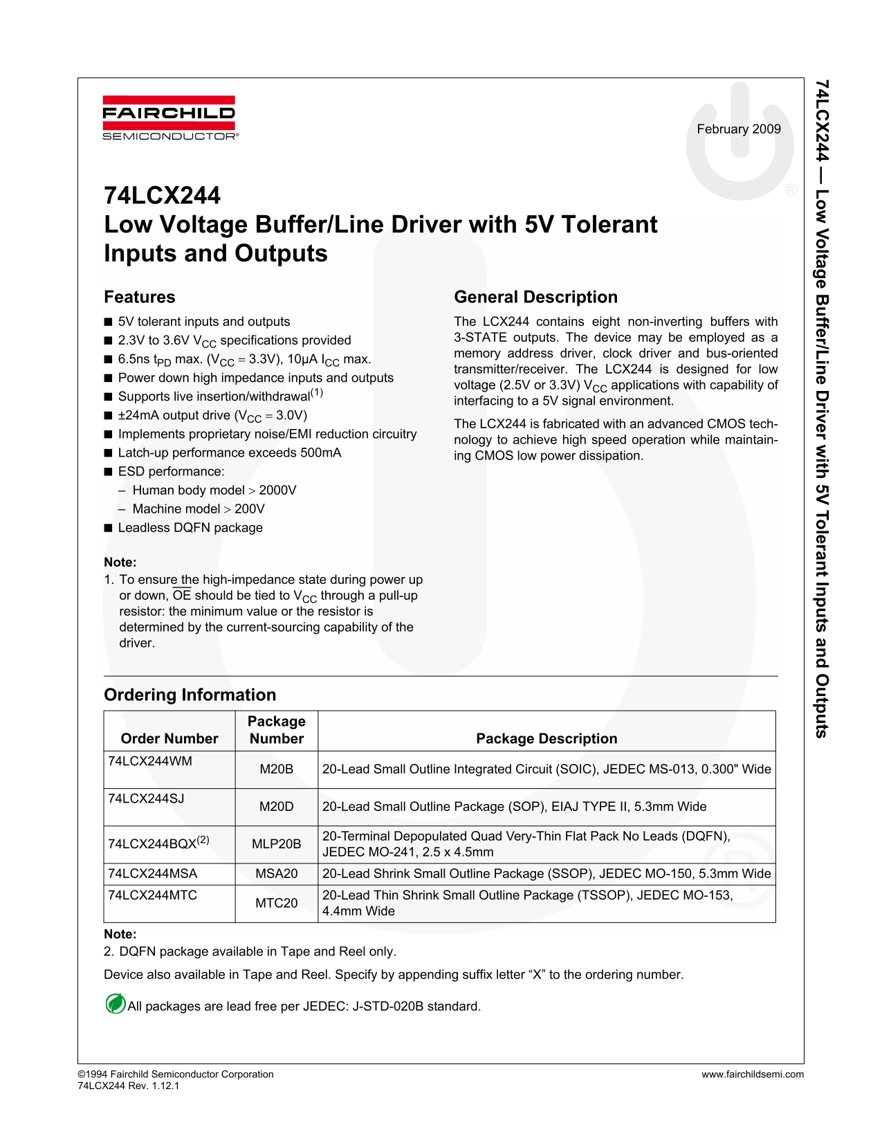
Fairchild Semiconductor 74LCX244 datasheet (February 2009) documenting this low voltage octal buffer/line driver with 3-STATE outputs and 5V tolerant inputs/outputs for mixed-voltage interfacing. Features 2.3V to 3.6V VCC operation, 6.5ns maximum propagation delay at 3.3V, +/-24mA output drive current, and proprietary noise/EMI reduction circuitry. Supports live insertion and withdrawal with power-down high-impedance inputs/outputs. Latch-up performance exceeds 500mA; ESD protection exceeds 2000
Page 1 Text Content
74LC X244 Low Voltage B uffer/Line D river w ith 5V Tolerant Inputs and O utputs
February 2009
74LCX244 Low Voltage Buffer/Line Driver with 5V Tolerant Inputs and Outputs Features General Description 5V tolerant inputs and outputs The LCX244 contains eight non-inverting buffers with
2.3V to 3.6V VCC specifications provided 3-STATE outputs. The device may be employed as a memory address driver, clock driver and bus-oriented
6.5ns t PD max. (VCC = 3.3V), 10µA ICC max.
transmitter/receiver. The LCX244 is designed for low
Power down high impedance inputs and outputs
voltage (2.5V or 3.3V) VCC applications with capability of
Supports live insertion/withdrawal(1)
interfacing to a 5V signal environment.
±24m A output drive (VCC = 3.0V)
The LCX244 is fabricated with an advanced CMOS tech-
Implements proprietary noise/EMI reduction circuitry
nology to achieve high speed operation while maintain-
Latch-up performance exceeds 500m A ing CMOS low power dissipation. ESD performance: Human body model > 2000V Machine model > 200V Leadless DQFN package
Note: 1. To ensure the high-impedance state during power up or down, OE should be tied to VCC through a pull-up resistor: the minimum value or the resistor is determined by the current-sourcing capability of the driver.
Ordering Information
Package
Order Number Number Package Description 74LCX244WM
M20B 20-Lead Small Outline Integrated Circuit (SOIC), JEDEC MS-013, 0.300" Wide
74LCX244SJ
M20D 20-Lead Small Outline Package (SOP), EIAJ TYPE II, 5.3mm Wide
20-Terminal Depopulated Quad Very-Thin Flat Pack No Leads (DQFN),
74LCX244BQX(2) MLP20B
JEDEC MO-241, 2.5 x 4.5mm
74LCX244MSA MSA20 20-Lead Shrink Small Outline Package (SSOP), JEDEC MO-150, 5.3mm Wide 74LCX244MTC 20-Lead Thin Shrink Small Outline Package (TSSOP), JEDEC MO-153,
MTC20
4.4mm Wide
Note: 2. DQFN package available in Tape and Reel only. Device also available in Tape and Reel. Specify by appending suffix letter X to the ordering number.
All packages are lead free per JEDEC: J-STD-020B standard.
©19 94 Fairchild Semiconductor Corporation www.fairchildsemi.com 74L CX244 Rev. 1.12.1
Page Summary Contents For Fairchild 74LC244 Data Handbook
Manual Details
| Brand | Fairchild |
|---|---|
| Pages | 14 |
| File Size | 717.18 KB |
| Published | July 06, 2026 |
Enter the captcha to get the download link:

Frequently Asked Questions
How should I configure the OE pin during power cycling?
To maintain a high-impedance state during power up or down, the OE pin must be tied to V through a pull-up resistor.
What is the maximum current the device can output?
The LCX244 supports an output drive capacity of ±24mA when operating at 3.0V.
Are there any limitations regarding voltage ratings?
While absolute maximum ratings exist, users should adhere to recommended operating conditions for optimal performance and reliability.
What must be done with unused input pins?
Unused inputs must be actively held HIGH or LOW states; they are not allowed to float.