Fairchild 74ABT16652 16-Bit Transceivers and Registers with 3-State Outputs - Data Manual
Summary
This 16-bit transceiver and register IC is engineered for reliable, high-speed management of dual A/B data buses. The device features dedicated registers and 3-STATE outputs, ensuring robust support for both real-time data streaming and stored data transfer. This manual serves as a comprehensive resource for system designers, providing detailed pin descriptions, functional operating tables, electrical specifications (e.g., setup time, propagation delay), and connection diagrams necessary for integrating the IC into complex digital bus architectures requiring precise control over data flow.
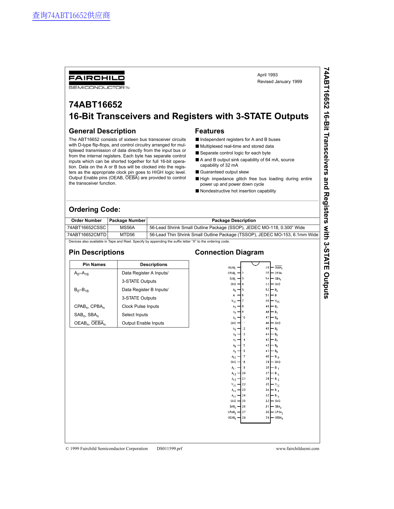
Page 1 Text Content
查询74ABT16652供应商
74A 16652 16-B it Tran sceivers an eg isters w ith 3-S TA tp ts
April 1993 Revised January 1999
74ABT16652 16-Bit Transceivers and Registers with 3-STATE Outputs General Description Features The ABT16652 consists of sixteen bus transceiver circuits Independent registers for A and B buses with D-type flip-flops, and control circuitry arranged for mul-
Multiplexed real-time and stored data
tiplexed transmission of data directly from the input bus or
Separate control logic for each byte
from the internal registers. Each byte has separate control
A and B output sink capability of 64 m A, source
inputs which can be shorted together for full 16-bit opera-
capability of 32 m A
tion. Data on the A or B bus will be clocked into the regis-
ters as the appropriate clock pin goes to HIGH logic level. Guaranteed output skew
Output Enable pins (OEAB, OEBA) are provided to control High impedance glitch free bus loading during entire the transceiver function. power up and power down cycle
Nondestructive hot insertion capability
Ordering Code: Order Number Package Number Package Description 74ABT16652CSSC MS56A 56-Lead Shrink Small Outline Package (SSOP), JEDEC MO-118, 0.300” Wide 74ABT16652CMTD MTD56 56-Lead Thin Shrink Small Outline Package (TSSOP), JEDEC MO-153, 6.1mm Wide Devices also available in Tape and Reel. Specify by appending the suffix letter “X” to the ordering code.
Pin Descriptions Connection Diagram Pin Names Descriptions
A0–A16 Data Register A Inputs/
3-STATE Outputs
B0–B16 Data Register B Inputs/
3-STATE Outputs
CPABn, CPBAn Clock Pulse Inputs
SABn, SBAn Select Inputs
OEABn, OEBAn Output Enable Inputs
© 1999 Fairchild Semiconductor Corporation DS011599.prf www.fairchildsemi.com
Page Summary Contents For Fairchild 74ABT16652 16-Bit Transceivers and Registers with 3-State Outputs - Data Manual
Manual Details
| Brand | Fairchild |
|---|---|
| Pages | 9 |
| File Size | 90.81 KB |
| Published | July 06, 2026 |
Enter the captcha to get the download link:

Frequently Asked Questions
What is the chip's maximum sink capability for an A or B bus segment?
Each byte has separate control logic supporting an output sink capacity of 64 mA.
Under what conditions do the bus lines maintain their last state?
If OEAB and OEBA are active, and all external data sources are in a HIGH impedance state, each bus set will remain at its last recorded state.
How does the device switch between real-time and stored data transmission?
The SAB and SBA select inputs control multiplexing, enabling simultaneous transfer of either real-time or internally stored data.
Is this chip suitable for use in critical life support applications?
Fairchild warns that its products are not authorized for use as critical components in life support systems without express written approval.