Fairchild Semiconductor 74ABT16374 16-Bit D-Type Flip-Flop with 3-State Outputs - Data Sheet & User Manual
Summary
Fairchild 74ABT16374 16-bit D-type flip-flop with 3-state outputs for bus-oriented applications. Features byte-controlled architecture for independent or 16-bit operation, edge-triggered buffered clock, high-impedance power transitions, and hot insertion. Covers truth tables, timing specs, and ratings for 48-lead SSOP/TSSOP packages with latch-up protection. For digital designers developing bus drivers, registers, and buffers in computing and communications.
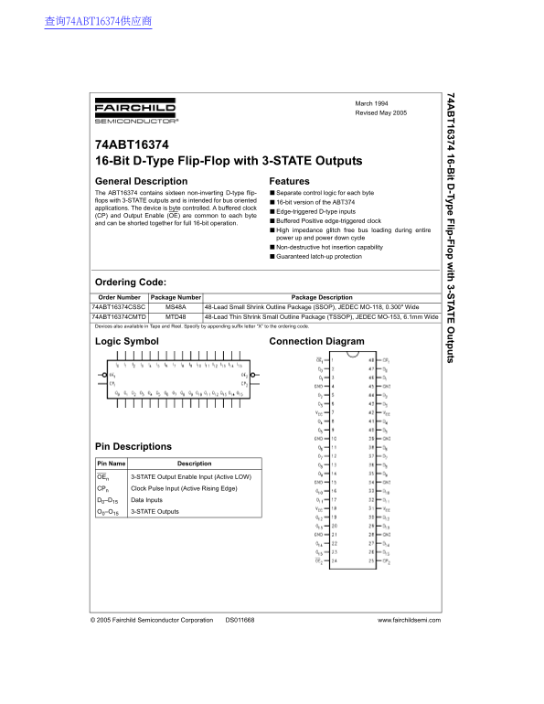
Page 1 Text Content
查询74ABT16374供应商
74A 16374 16-B it D -Typ e F lip -F lo ith 3-S TA tp ts
March 1994 Revised May 2005
74ABT16374 16-Bit D-Type Flip-Flop with 3-STATE Outputs General Description Features The ABT16374 contains sixteen non-inverting D-type flip- ■Separate control logic for each byte flops with 3-STATE outputs and is intended for bus oriented
■16-bit version of the ABT374
applications. The device is byte controlled. A buffered clock
■Edge-triggered D-type inputs
(CP) and Output Enable (OE) are common to each byte
■Buffered Positive edge-triggered clock
and can be shorted together for full 16-bit operation.
■High impedance glitch free bus loading during entire power up and power down cycle ■Non-destructive hot insertion capability ■Guaranteed latch-up protection
Ordering Code: Order Number Package Number Package Description 74ABT16374CSSC MS48A 48-Lead Small Shrink Outline Package (SSOP), JEDEC MO-118, 0.300" Wide 74ABT16374CMTD MTD48 48-Lead Thin Shrink Small Outline Package (TSSOP), JEDEC MO-153, 6.1mm Wide Devices also available in Tape and Reel. Specify by appending suffix letter “X” to the ordering code.
Logic Symbol Connection Diagram
Pin Descriptions Pin Name Description
OEn 3-STATE Output Enable Input (Active LOW)
CPn Clock Pulse Input (Active Rising Edge)
D0–D15 Data Inputs
O0–O15 3-STATE Outputs
© 2005 Fairchild Semiconductor Corporation DS011668 www.fairchildsemi.com
Page Summary Contents For Fairchild Semiconductor 74ABT16374 16-Bit D-Type Flip-Flop with 3-State Outputs - Data Sheet & User Manual
Manual Details
| Brand | Fairchild |
|---|---|
| Pages | 6 |
| File Size | 85.27 KB |
| Published | June 17, 2026 |
Enter the captcha to get the download link:

Frequently Asked Questions
What package options are available for the 74ABT16374?
It comes in a 48-Lead SSOP (MO-118) or a 48-Lead TSSOP (MO-153) package.
How do I enable the outputs on the 74ABT16374?
Set the Output Enable (OE) pin LOW to enable the outputs; a HIGH input puts them in a high impedance (3-STATE) state.
What is the maximum recommended supply voltage?
The absolute maximum supply voltage is 5.5V; the recommended operating range is 4.5V to 5.5V.
What are the setup time requirements for the data inputs?
The data (D) setup time before the clock's rising edge is a minimum of 1.1 ns for both HIGH and LOW signals.