# A B C D E F G H I J K L M N O P Q R S T U V W X Y Z

ANALOG DEVICES Ultralow Noise VGAs with Preamplifier and Programmable RIN AD8331 AD8332 User Manual - Specifications

Summary

These single- and dual-channel Variable Gain Amplifiers are designed for high-performance signal integrity across frequencies up to 120 MHz in ultra-low noise environments. The product features a combined LNA preamplifier, an X-AMP VGA with a wide 48 dB gain range, and a programmable postamplifier optimized for accurate data acquisition. This manual provides comprehensive details on the device architecture, applications (including ultrasound, sonar, and high-speed ADC driving), and precise operational guidelines necessary for reliable signal processing in demanding electronic systems.
📄 Preview 📖 Table of Contents Contents PAGE OF 32

Page 1 Text Content

Ultralow Noise VGAs with

Preamplifier and Programmable RIN

AD8331/AD8332

FUNCTIONAL BLOCK DIAGRAM

FEATURES

VIN1VIP1LOP1LON1 VPSV HILOVCM2VCM1

Ultralow noise preamplifier

Voltage noise = 0.74 n V/√Hz VPS1

Current noise = 2.5 p A/√Hz COM1

+19d B [(–48 to 0) + 21] d B

3 d B bandwidth: 120 MHz

INH1 POST

Low power: 125 m W/channel VGA 1

LNA 1 AMP1

Wide gain range with programmable postamp

–4.5 d B to +43.5 d B BIAS BIAS AND GAIN

(VMID) INTERPOLATOR INT

+7.5 d B to +55.5 d B

LMD2 VOL2

Low output-referred noise: 48 n V/√Hz typical POST

LNA 2 VGA 2

Active input impedance matching VOH2

Optimized for 10-/12-bit ADCs VPS2

CLAMP

Selectable output clamping level

6COM2

Single 5 V supply operation

VIN2VIP2LOP2LON2 ENB RCLMPCOMM

Available in space-saving chip scale package

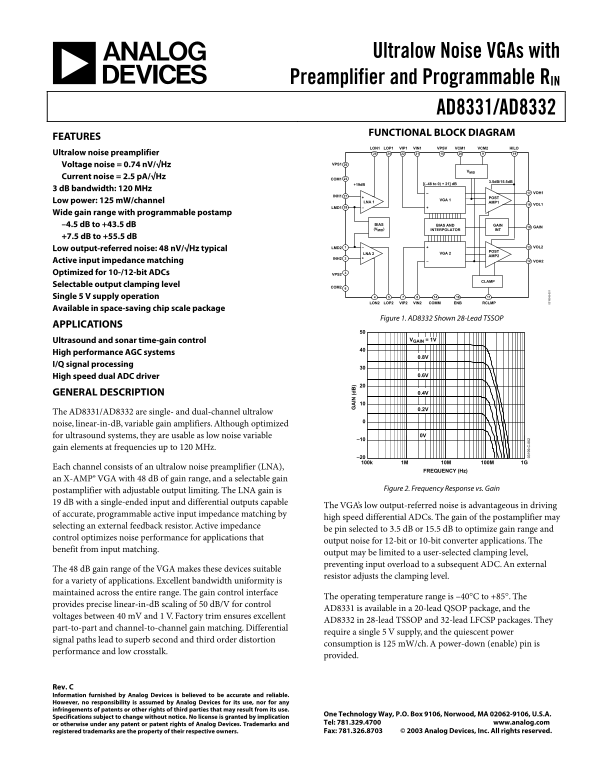
Figure 1. AD8332 Shown 28-Lead TSSOP

APPLICATIONS

Ultrasound and sonar time-gain control VGAIN = 1V

High performance AGC systems IN (d

I/Q signal processing

High speed dual ADC driver 0.6V

GENERAL DESCRIPTION 0.4V

The AD8331/AD8332 are single- and dual-channel ultralow noise, linear-in-d B, variable gain amplifiers. Although optimized

for ultrasound systems, they are usable as low noise variable 0V

gain elements at frequencies up to 120 MHz.

Each channel consists of an ultralow noise preamplifier (LNA),

FREQUENCY (Hz)

an X-AMP® VGA with 48 d B of gain range, and a selectable gain

Figure 2. Frequency Response vs. Gain

postamplifier with adjustable output limiting. The LNA gain is 19 d B with a single-ended input and differential outputs capable

The VGA’s low output-referred noise is advantageous in driving

of accurate, programmable active input impedance matching by

high speed differential ADCs. The gain of the postamplifier may

selecting an external feedback resistor. Active impedance 9- -0

be pin selected to 3.5 d B or 15.5 d B to optimize gain range and

control optimizes noise performance for applications that

output noise for 12-bit or 10-bit converter applications. The

benefit from input matching. 9- B-

output may be limited to a user-selected clamping level, preventing input overload to a subsequent ADC. An external

The 48 d B gain range of the VGA makes these devices suitable

resistor adjusts the clamping level.

for a variety of applications. Excellent bandwidth uniformity is maintained across the entire range. The gain control interface

The operating temperature range is –40°C to +85°. The

provides precise linear-in-d B scaling of 50 d B/V for control

AD8331 is available in a 20-lead QSOP package, and the

voltages between 40 m V and 1 V. Factory trim ensures excellent

AD8332 in 28-lead TSSOP and 32-lead LFCSP packages. They

part-to-part and channel-to-channel gain matching. Differential

require a single 5 V supply, and the quiescent power

signal paths lead to superb second and third order distortion

consumption is 125 m W/ch. A power-down (enable) pin is

performance and low crosstalk.

provided.

Rev. C Information furnished by Analog Devices is believed to be accurate and reliable. However, no responsibility is assumed by Analog Devices for its use, nor for any infringements of patents or other rights of third parties that may result from its use.

One Technology Way, P.O. Box 9106, Norwood, MA 02062-9106, U.S.A.

Specifications subject to change without notice. No license is granted by implication

or otherwise under any patent or patent rights of Analog Devices. Trademarks and Tel: 781.329.4700 www.analog.com registered trademarks are the property of their respective owners. Fax: 781.326.8703 © 2003 Analog Devices, Inc. All rights reserved.

Page Summary Contents For ANALOG DEVICES Ultralow Noise VGAs with Preamplifier and Programmable RIN AD8331 AD8332 User Manual - Specifications

Page 1 Ultralow Noise VGAs with Preamplifier and Programmable RIN AD8331/AD8332 FUNCTIONAL BLOCK DIAGRAM FEATURES VIN1VIP1LOP1LON1 VPSV HILOVCM2VCM1 Ultralow noise preamplifier Voltage noise = 0.74 n V/√Hz V...
Page 2 AD8331/AD8332 LNA – External Components TABLE OF CONTENTS Driving ADCs REVISION HISTORY.................................................................. Overload AD8331, AD8332—Specifications...........
Page 3 AD8331/AD8332 AD8331, AD8332—SPECIFICATIONS Table 1. TA = 25°C, VS = 5 V, RL = 500 Ω, RS = RIN = 50 Ω, RFB = 280 Ω, CSH = 22 p F, f = 10 MHz, RCLMP = ∞, CL = 1 p F, VCM pin floating, –4.5 d B to +43.5...
Page 4 AD8331/AD8332 Parameter Conditions Min Typ Max Unit Harmonic Distortion VGAIN = 0.5 V, VOUT = 1 V p-p HD2 –88 d Bc f = 1 MHz HD3 –85 d Bc HD2 –68 d Bc f = 10 MHz HD3 –65 d Bc Input 1 d B Compression P...
Page 5 AD8331/AD8332 Parameter Conditions Min Typ Max Unit OUTPUT CLAMP INTERFACE (Pin RCLMP; HI or LO Gain) Accuracy HILO = LO RCLMP = 2.74 kΩ, VOUT = 1 V p-p (Clamped) ±50 m V HILO = HI RCLMP = 2.21 kΩ, VO...
Page 6 AD8331/AD8332 ABSOLUTE MAXIMUM RATINGS Table 2. Absolute Maximum Ratings Parameter Rating Stresses above those listed under the Absolute Maximum Voltage Ratings may cause permanent damage to the devic...
Page 7 AD8331/AD8332 IN (d IN (d IN (d AD8331, AD8332—TYPICAL PERFORMANCE CHARACTERISTICS TA = 25°C, VS = 5 V, RL = 500 Ω, RS = RIN = 50 Ω, RFB = 280 Ω, CSH = 22 p F, f = 10 MHz, RCLMP = ∞, CL = 1 p F, VCM =...
Page 8 AD8331/AD8332 IN (d IN (d IN (d VGAIN = 1V VOUT = 1 V p-p –10 0.2V VGAIN = 1V FREQUENCY (Hz) FREQUENCY (Hz) Figure 9. Frequency Response for Various Values of VGAIN, HILO = HI Figure 12. Channel-to-Ch...
Page 9 AD8331/AD8332 IN PU IM PE (Ω TP IM PE (Ω SAMPLE SIZE = 100 0.2V < VGAIN < 0.7V 25j f = 100k Hz RIN = 50Ω RFB = 270Ω RIN = 75Ω, RFB = 412Ω RIN = 100Ω, RFB = 549Ω RIN = 200Ω, RFB = 1.1kΩ 49.7 49.8...
Page 10 AD8331/AD8332 IN PU IS (n V/ z) IN PU IS (n V/ z) TP T- EF ER ED IS (n V/ z) RS = 0, RFB = ∞, f = 10MHz 0.95 VGAIN = 1V, f = 10MHz HILO = HI 0.70 HILO = LO 0.2 0.4 0.8 1.00.6 –10 10–30–50 VGAIN (V) TE...
Page 11 AD8331/AD8332 IC IS TO TI (d c) IS FI (d IS FI (d f = 10MHz, RS = 50Ω f = 10MHz VOUT = 1V p-p HILO = LO, RIN = 50Ω HILO = LO, –50 HD3 HILO = HI, RIN = 50Ω HILO = LO, –60 HD2 HILO = LO, RFB HILO = HI, ...
Page 12 AD8331/AD8332 IN PU PO ER IS TO TI (d c) IS TO TI (d c) VOUT = 1V p-p COMPOSITE (f1 + f2) VOUT = 1V p-p INPUT RANGE –20 LIMITED WHEN –40 HILO LO HILO LO, –30 HILO LO, –60 HILO HI, HD2 –50 HILO HI, HD3...
Page 13 AD8331/AD8332 HILO = HI HILO = LO 500m V 10ns Figure 39. Large Signal Pulse Response, G = 30 d B, RCLMP (kΩ) HILO = HI or LO, Top: Input, Bottom: Output Voltage 9- B- Figure 42. Clamp Level vs. RCLMP ...
Page 14 AD8331/AD8332 100ns 1V Figure 45. VGA Overdrive Recovery, VINH 4 m V p-p to 70 m V p-p Burst, Figure 48. Enable Response, Large Signal, VGAIN = 1 V, VGA Output Shown Attenuated 24 d B 9- B- Top: VENB,...
Page 15 AD8331/AD8332 TEST CIRCUITS NETWORK ANALYZER INOUT 22p F DUT 1:1 *FERRITE BEAD Figure 51. Gain and Bandwidth Measurements OSCILLOSCOPE FB* 237Ω 50Ω INH 9- -0 28Ω IN 22p F DUT 1:1 *FERRITE BEAD Figure ...
Page 16 AD8331/AD8332 SPECTRUM ANALYZER FB* 237Ω 28Ω IN DUT 1:1 22p F LMD 50Ω *FERRITE BEAD Figure 54. Distortion NETWORK ANALYZER INOUT 50Ω FB* 237Ω 22p F DUT *FERRITE BEAD Figure 55. S11 Measurements Rev. C...
Page 17 AD8331/AD8332 THEORY OF OPERATION OVERVIEW MODE HI The following discussion applies to all part numbers. Figure 56 (WHERE AVAILABLE) and Figure 1 are functional block diagrams of the AD8331 and HILO H...
Page 18 AD8331/AD8332 CFB is needed in series with RFB, since the dc levels at Pins LON A simplified schematic of the LNA is shown in Figure 59. INH and INH are unequal. Expressions for choosing RFB in terms ...
Page 19 AD8331/AD8332 IS (d IS FI (d UNTERMINATED The primary purpose of input impedance matching is to RS improve the system transient response. With resistive termination, the input noise increases due to t...
Page 20 AD8331/AD8332 X-AMP VGA Gain control response time is less than 750 ns to settle within 10% of the final value for a change from minimum to max- The input of the VGA is a differential R-2R ladder atte...
Page 21 AD8331/AD8332 Gain control noise is a concern in very low noise applications. Thermal noise in the gain control interface can modulate the VOH channel gain. The resultant noise is proportional to the ...
Page 22 AD8331/AD8332 0.1µF LNA APPLICATIONS FB SOURCE LMD2 LMD1 0.1µF LNA – EXTERNAL COMPONENTS INH2 INH1 The LMD pin (connected to the bias circuitry) must be CFB* 1n F 5V+5V bypassed to ground, and signal ...
Page 23 AD8331/AD8332 Gain Input Logic Inputs—ENB, MODE, and HILO Pin GAIN is common to both channels of the AD8332. The The input impedance of all enable pins is nominally 25 kΩ and input impedance is nomina...
Page 24 AD8331/AD8332 Table 4. Clamp Resistor Values The relative noise and distortion performance of the two gain Clamp Resistor Value (kΩ) Clamp Level modes can be compared in Figure 21 and Figure 27 throug...
Page 25 AD8331/AD8332 IN (d POSTAMP X-AMP POSTAMP X-AMP OVERLOAD OVERLOAD OVERLOAD OVERLOAD LAYOUT, GROUNDING, AND BYPASSING Due to their excellent high frequency characteristics, these devices are sensitive ...
Page 26 AD8331/AD8332 NC LMD COMM MEASUREMENT CONSIDERATIONS AD8331 Figure 51 through Figure 55 show typical measurement configurations and proper interface values for measurements NC INH ENBL with 50 Ω condi...
Page 27 AD8331/AD8332 S3 EIN2 AD8332ARU 28LMD1 0.1µF LMD2C49 C70 TP6 TP3 L13 C60 +5V 120n H FB (RED) 120n H FB 0.1µF TB1 27INH1 S1 +5V C79 EIN1 C80 JP5 JP6 CFB2 22 PF C46 22PF IN2 IN1 CFB1 TP4 1µF 18n F (BLAC...
Page 28 AD8331/AD8332 VR1 ADP3339AKC-3.3 +3.3VAVDD C44 120n H FB 1µF +3.3VCLK ADCLK IN OUT GND L4 R11 120n H FB 100ΩR10 +3.3VADDIG 10µF 6.3V JP 2 AGND AVDD 0Ω R5 SHARED OUT C30 33Ω REF TAB VIN+_A VIN+_A CLK_A...
Page 29 AD8331/AD8332 +3.3VDVDD DATACLKA G1 U10 VCC 22Ω 74VHC541 C3 C28 G2 GND 0.1µF 10µF RP 9 RP 1 OTR_A EA A2 ER LE Y2 SH EA ER LE SH RP 10 RP2 +3.3VDVDD G1 U7 VCC 74VHC541 C8 C10 C76 × 4 G2 GND 0.1µF 0.1µF...
Page 30 AD8331/AD8332 PIN CONFIGURATION AND FUNCTION DESCRIPTIONS AD8331 PIN 1 COMM IDENTIFIER INH ENBL VPSL ENBV LON COMM AD8331 LOP TOP VIEW VOL (Not to Scale) COML VOH VIP VPOS VIN HILO MODE RCLMP 9- -0 GA...
Page 31 AD8331/AD8332 AD8332 LMD2 PIN 1 LMD1 IDENTIFIER INH2 INH1 VPS2 VPS1 LON1 PIN 1 COMM LON2 LON1 INDICATOR VPS1 VOH1 LOP2 LOP1 INH1 VOL1 AD8332 AD8332 LMD1 VPSV COM2 COM1 TOP VIEW TOP VIEW (Not to Scale)...
Page 32 AD8331/AD8332 OUTLINE DIMENSIONS 9.70 BSC 0.154 BSC 4.50 BSC 4.40 4.30 PIN 1 6.40 BSC PIN 1 0.065 0.069 0.65 BSC 1.20 MAX 0.025 0.012 SEATING 0° BSC 0.008 0.010 8° 0.75 PLANE 0.016 0° 0.60 COPLANARITY...

Manual Details

Brand Analog Devices
Pages 32
File Size 482.99 KB
Published June 15, 2026
5 views

Enter the captcha to get the download link:

captcha

Frequently Asked Questions

What are the operating temperature limits for these amplifiers?

The device operates within a temperature range of –40°C to +85°C.

How is input overload protection implemented for ADCs?

The output can be limited to a user-selected clamping level, which adjusts by selecting an external resistor.

What voltage supply does the amplifier require?

They require a single 5 V supply for operation.

To optimize gain range and noise performance, what adjustment is necessary?

Select an external feedback resistor to adjust the postamplifier gain or select specific input impedance matching settings (3.5 dB or 15.5 dB).

What is the maximum frequency range supported by the amplifiers?

They are usable at frequencies up to 120 MHz.