# A B C D E F G H I J K L M N O P Q R S T U V W X Y Z

AD7147 Analog Devices User's Manual and Specifications

Summary

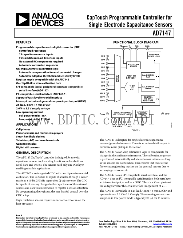
The AD7147 is a high-resolution Capacitance-to-Digital Converter (CDC) designed for sensing changes in capacitance using up to 13 inputs. Featuring automatic on-chip calibration and low power consumption, it provides highly accurate touch and environmental detection vital for smart devices, mobile applications, and embedded controls. This manual guides engineers through the full technical specifications, operational modes (SPI/I²C), functional block diagram, and advanced setup required for seamless integration into demanding electronics designs.
📄 Preview 📖 Table of Contents Contents PAGE OF 72

Page 1 Text Content

Cap Touch Programmable Controller for Single-Electrode Capacitance Sensors

AD7147 FEATURES FUNCTIONAL BLOCK DIAGRAM

ACSHIELD VCC GND BIAS

Programmable capacitance-to-digital converter (CDC) Femtofarad resolution

13 capacitance sensor inputs POWER-ON

19CIN0 RESET LOGIC

9 ms update rate, all 13 sensor inputs

20CIN1

No external RC components required

21CIN2

EXCITATION

Automatic conversion sequencer

SOURCE

22CIN3

On-chip automatic calibration logic

23CIN4

Automatic compensation for environmental changes

24CIN5

CALIBRATION

Automatic adaptive threshold and sensitivity levels AD7147/

1CIN6 AD7147-1

Register map is compatible with the AD7142

2CIN7

On-chip RAM to store calibration data

3CIN8 16-BIT

SPI-compatible (serial-peripheral-interface-compatible) CALIBRATION

ENGINE

4CIN9 CDC

serial interface (AD7147)

5CIN10

I2C-compatible serial interface (AD7147-1)

6CIN11 CONTROL

Separate VDRIVE level for serial interface

AND DATA

7CIN12 REGISTERS

Interrupt output and general-purpose input/output (GPIO) 24-lead, 4 mm × 4 mm LFCSP 2.6 V to 3.3 V supply voltage

Low operating current INTERRUPT

SERIAL INTERFACE

VDRIVE AND GPIO GPIO

AND CONTROL LOGIC

Full power mode: 1 m A LOGIC

SW IT Low power mode: 21.5 μA TR IX

www.BDTIC.com/ADI

APPLICATIONS SDO/ SDI/ SCLK CS/ INT SDA ADD0 ADD1

Cell phones Figure 1. Personal music and multimedia players Smart handheld devices

Television, A/V, and remote controls The AD7147 is designed for single electrode capacitance Gaming consoles sensors (grounded sensors). There is an active shield output to Digital still cameras minimize noise pickup in the sensor. The AD7147 has on-chip calibration logic to compensate for

GENERAL DESCRIPTION

changes in the ambient environment. The calibration sequence

The AD7147 Cap Touch™ controller is designed for use with

is performed automatically and at continuous intervals as long

capacitance sensors implementing functions such as buttons,

as the sensors are not touched. This ensures that there are no

scroll bars, and wheels. The sensors need only one PCB layer,

false or nonregistering touches on the external sensors due to

enabling ultrathin applications.

a changing environment.

The AD7147 is an integrated CDC with on-chip environmental

The AD7147 has an SPI-compatible serial interface, and the

calibration. The CDC has 13 inputs channeled through a switch

AD7147-1 has an I2C®-compatible serial interface. Both parts have

matrix to a 16-bit, 250 k Hz sigma-delta (∑-Δ) converter. The CDC

an interrupt output, as well as a GPIO. There is a VDRIVE pin to set

is capable of sensing changes in the capacitance of the external

the voltage level for the serial interface independent of VCC.

sensors and uses this information to register a sensor activation.

The AD7147 is available in a 24-lead, 4 mm × 4 mm LFCSP and

By programming the registers, the user has full control over the

operates from a 2.6 V to 3.6 V supply. The operating current con-

CDC setup.

sumption in low power mode is typically 26 μA for 13 sensors.

High resolution sensors require minor software to run on the host processor.

Rev. A Information furnished by Analog Devices is believed to be accurate and reliable. However, no responsibility is assumed by Analog Devices for its use, nor for any infringements of patents or other

One Technology Way, P.O. Box 9106, Norwood, MA 02062-9106, U.S.A.

rights of third parties that may result from its use. Specifications subject to change without notice. No

license is granted by implication or otherwise under any patent or patent rights of Analog Devices. Tel: 781.329.4700 www.analog.com Trademarks and registered trademarks are the property of their respective owners. Fax: 781.461.3113 ©2007–2008 Analog Devices, Inc. All rights reserved.

Page Summary Contents For AD7147 Analog Devices User's Manual and Specifications

Page 1 Cap Touch Programmable Controller for Single-Electrode Capacitance Sensors AD7147 FEATURES FUNCTIONAL BLOCK DIAGRAM ACSHIELD VCC GND BIAS Programmable capacitance-to-digital converter (CDC) Femtofarad...
Page 2 AD7147 TABLE OF CONTENTS Features .............................................................................................. 1  Capacitance Sensor Behavior Without Calibration ............... 23  ...
Page 3 AD7147 SPECIFICATIONS VCC = 2.6 V to 3.6 V, TA = −40o C to +85°C, unless otherwise noted. Table 1. Parameter Min Typ Max Unit Test Conditions/Comments CAPACITANCE-TO-DIGITAL CONVERTER Update Rate 8.73...
Page 4 AD7147 AVERAGE CURRENT SPECIFICATIONS Table 2. Typical Average Current in Low Power Mode1 Low Power Decimation Current Values of Conversion Stages (μA) Mode Delay Rate 1 2 3 4 5 6 7 8 9 10 11 12 200 m...
Page 5 AD7147 SPI TIMING SPECIFICATIONS (AD7147) TA = −40°C to +85°C, sample tested at 25°C to ensure compliance. VDRIVE = 1.65 V to 3.6 V, and VCC = 2.6 V to 3.6 V, unless otherwise noted. All input signals...
Page 6 AD7147 I2C TIMING SPECIFICATIONS (AD7147-1) TA = −40°C to +85°C, sample tested at 25°C to ensure compliance. VDRIVE = 1.65 V to 3.6 V, and VCC = 2.6 V to 3.6 V, unless otherwise noted. All input signa...
Page 7 AD7147 ABSOLUTE MAXIMUM RATINGS Table 6. Stresses above those listed under Absolute Maximum Ratings Parameter Rating may cause permanent damage to the device. This is a stress VCC to GND −0.3 V to +3....
Page 8 AD7147 PIN CONFIGURATIONS AND FUNCTION DESCRIPTIONS IN IN PIN 1 PIN 1 SH IE LD IN INDICATOR1CIN6 GPIO INDICATOR1CIN6 GPIO IA IN 2CIN7 INT 2CIN7 INT IN 3CIN8 AD7147 CS 3CIN8 AD7147-1 ADD1 IN 4CIN9 TOP ...
Page 9 AD7147 TYPICAL PERFORMANCE CHARACTERISTICS 200ms DECIMATION = 64 400ms DECIMATION = 128 600ms DECIMATION = 256 800ms VCC (V) VCC (V) Figure 7. Supply Current vs. Supply Voltage 3- 3- Figure 10. Low Po...
Page 10 AD7147 (µ (µ ACSHIELD CAPACITIVE LOAD (p F) SINE WAVE FREQUENCY (Hz) Figure 13. Output Code vs. Capacitive Load on ACSHIELD Figure 16. Power Supply Sine Wave Rejection, VCC = 3.6 V IN PU PA IT (p F) I...
Page 11 AD7147 THEORY OF OPERATION The AD7147 and AD7147-1 are CDCs with on-chip environ- require low power operation to provide the user with significant mental compensation. They are intended for use in por...
Page 12 TP ES AD7147 Registering a Sensor Activation Complete Solution for Capacitance Sensing When a user approaches a sensor, the total capacitance associated Analog Devices, Inc., provides a complete solut...
Page 13 AD7147 Full Power Mode settings. See the CDC Conversion Sequence Time section for more information.) In full power mode, all sections of the AD7147 remain fully powered and converting at all times. Wh...
Page 14 AD7147 CAPACITIANCE-TO-DIGITAL CONVERTER The capacitance-to-digital converter on the AD7147 has a Σ-Δ from midscale, decrease the POS_AFE_OFFSET or architecture with 16-bit resolution. There are 13 po...
Page 15 AD7147 A button sensor generally requires one sequencer stage; this is A wheel sensor requires eight stages, whereas a slider requires two shown in Figure 26 as B1. However, it is possible to configur...
Page 16 AD7147 CDC CONVERSION SEQUENCE TIME Table 10. CDC Conversion Times for Full Power Mode Conversion Time (ms) SEQUENCE_STAGE_NUM Decimation = 64 Decimation = 128 Decimation = 256 0 0.768 1.536 3.072 1 1...
Page 17 AD7147 CAPACITANCE SENSOR INPUT CONFIGURATION Each input connection from the external capacitance sensors to To connect CIN0 to the positive CDC input and CIN12 to the the converter of the AD7147 can ...
Page 18 AD7147 NONCONTACT PROXIMITY DETECTION The AD7147 internal signal processing continuously monitors by the PROXIMITY_RECAL_LVL bits for a set period of time all capacitance sensors for noncontact proxim...
Page 19 AD7147 Table 12. Proximity Control Registers (See Figure 34) Length Bit Name (Bits) Register Address Description FP_PROXIMITY_CNT 4 0x002[7:4] Calibration disable time in full power mode. LP_PROXIMITY...
Page 20 AD7147 USER APPROACHES SENSOR t RECAL MEASURED CDC VALUE > STORED AMBIENT USER LEAVES BY PROXIMITY_RECAL _LVL SENSOR AREA t CONV_FP CDC CONVERSION SEQUENCE (INTERNAL) t CALDIS PROXIMITY DETECTION (...
Page 21 AD7147 FF_SKIP_CNT Determining the FF_SKIP_CNT value is required only once during the initial setup of the capacitance sensor interface. The proximity detection fast FIFO is used by the on-chip logic ...
Page 22 AD7147 FP_PROXIMITY_CNT LP_PROXIMITY_CNT CDC REGISTER 0x002 REGISTER 0x002 STAGEx_FF_WORD0 STAGEx_FF_WORD1 COMPARATOR 1 PROXIMITY 1 PROXIMITY |WORD0 – WORD3| PROXIMITY TIMING STAGEx_FF_WORD2 CONTROL L...
Page 23 AD7147 ENVIRONMENTAL CALIBRATION The AD7147 provides on-chip capacitance sensor calibration to SENSOR 1 INT ASSERTED automatically adjust for environmental conditions that have an STAGEx_HIGH_THRESHOL...
Page 24 TP ES AD7147 THRESHOLD EQUATIONS On-Chip Logic Stage High Threshold ⎛+= HIGHOFFSETSTAGEx AMBIENTSFSTAGEx THRESHOLDHIGHSTAGEx +⎟ HIGHOFFSETSTAGEx HIGHOFFSETSTAGEx (1) YSENSITIVITTHRESHOLDPOS On-Chip Lo...
Page 25 AD7147 SLOW_FILTER_UPDATE_LVL than the value of SLOW_FILTER_UPDATE_LVL. This variable is in Ambient Control Register 1 (AMB_COMP_CTRL1) The SLOW_FILTER_UPDATE_LVL controls whether the most (Address 0x...
Page 26 TP ES AD7147 ADAPTIVE THRESHOLD AND SENSITIVITY The AD7147 provides an on-chip, self-adjusting adaptive results in a large average maximum or minimum value, whereas threshold and sensitivity algorithm...
Page 27 AD7147 STAGEx_MAX_WORD0 STAGEx_MAX_WORD1 BANK 3 REGISTERS STAGEx_MAX_WORD2 STAGEx_MAX_WORD3 MAXIMUM 16Σ-Δ STAGEx_MAX_AVG LEVEL 16-BIT BANK 3 REGISTERS DETECTION LOGIC STAGEx_MAX_TEMP BANK 3 REGISTERS ...
Page 28 AD7147 INTERRUPT OUTPUT SENSOR-TOUCH INTERRUPT The AD7147 has an interrupt output that triggers an interrupt service routine on the host processor. The INT signal is on The sensor-touch interrupt mode...
Page 29 AD7147 CONVERSIONS STAGE0 STAGE1 STAGE2 STAGE3 STAGE4 STAGE5 STAGE6 STAGE7 STAGE8 STAGE9 STAGE10 STAGE11 SERIAL READS NOTES THIS IS AN EXAMPLE OF A CDC CONVERSION-COMPLETE INTERRUPT. THIS TIMING EXAMP...
Page 30 AD7147 GPIO INT OUTPUT CONTROL interrupt. This bit is set to 1 when the GPIO has triggered INT. The bit is cleared upon reading the GPIO_INT_STATUS bit if the The INT output signal can be controlled b...
Page 31 AD7147 SERIAL SERIAL READBACK READBACK GPIO INPUT LOW WHEN REGISTER IS READ BACK GPIO INPUT LOW WHEN REGISTER IS READ BACK INPUT INPUT INT INT OUTPUT OUTPUT GPIO INPUT HIGH WHEN REGISTER IS READ BACK ...
Page 32 AD7147 SE SO OUTPUTS ACSHIELD OUTPUT When the GPIO is configured as an output, the voltage level on the pin is set to either a low level or a high level, as defined by The AD7147 measures capacitance ...
Page 33 AD7147 SERIAL INTERFACE The AD7147 is available with an SPI-compatible interface. The Bits[15:11] of the command word must be set to 11100 to AD7147-1 is available with an I2C-compatible interface. Bo...
Page 34 AD7147 16-BIT COMMAND WORD DATA FOR STARTING DATA FOR NEXT ENABLE WORD R/W STARTING REGISTER ADDRESS REGISTER ADDRESS REGISTER ADDRESS CW CW CW CW CW CW CW CW CW CW CW CW CW CW CW CW SDI D15 D14 D0 D1...
Page 35 AD7147 16-BIT COMMAND WORD ENABLE WORD R/W REGISTER ADDRESS CW CW CW CW CW CW CW CW CW CW CW CW CW CW CW CW SDI XX XX XXX XXX XXX XXX XXX XXX XXX XXX XXX XXX XXX XXX XXX XXXSDO XXX D15 D14 D0 D15 D1 D...
Page 36 AD7147 START AD7147-1 DEVICE ADDRESS REGISTER ADDRESS [A15:A8] REGISTER ADDRESS [A7:A0] DEV DEV DEV DEV DEV DEV DEV R/W ACK A15 A14 A9 A8 ACK A7 A6 A1 A0 A6 A5 A4 A3 A2 A1 A0 STOP START REGISTER DATA ...
Page 37 AD7147 START AD7147-1 DEVICE ADDRESS REGISTER ADDRESS [A15:A8] REGISTER ADDRESS [A7:A0] DEV DEV DEV DEV DEV DEV DEV R/W ACK A15 A14 A9 A8 ACK A7 A6 A1 A0 ACK A6 A5 A4 A3 A2 A1 A0 SR AD7147-1 DEVICE AD...
Page 38 AD7147 PCB DESIGN GUIDELINES CAPACITIVE SENSOR BOARD MECHANICAL SPECIFICATIONS Table 19. Parameter Symbol Min Typ Max Unit Distance from Edge of Any Sensor to Edge of Grounded Metal Object D1 0.1 mm D...
Page 39 AD7147 POWER-UP SEQUENCE To power up the AD7147, use the following sequence when Address 0x004 = 832 initially developing the AD7147 and microprocessor serial Address 0x005 = interrupt enable register...
Page 40 AD7147 EC PL SE SO TO SH IE LD TYPICAL APPLICATION CIRCUITS SL ID ER VDRIVE HOST WITH SPI CIN6 GPIO 2.2kΩ INTERFACE BUTTON BUTTON CIN7 INT INT SCROLL CIN8 CS SS WHEEL AD7147 CIN9 SCLK SCK BUTTON CIN10...

Manual Details

Brand Analog Devices
Pages 72
File Size 1.30 MB
Published May 14, 2026
140 views

Enter the captcha to get the download link:

captcha

Frequently Asked Questions

How does the chip compensate for environmental changes?

It uses on-chip calibration logic that automatically performs adjustments to compensate for ambient environment changes continuously.

What is the low power consumption rate for operation?

The operating current in low power mode is typically 21.5 μA (or 26 μA if all 13 sensors are used).

How many capacitive inputs does the AD7147 support?

It has 13 capacitance sensor inputs, suitable for functions like buttons and scroll bars.