AD8675 Analog Devices Data Handbook and Specifications manual
Summary
A high-precision operational amplifier engineered for demanding instrumentation requiring utmost accuracy. Featuring ultra-low offset voltage, minimal current noise, and a reliable rail-to-rail output swing, this component maintains performance across extreme industrial temperatures (-40°C to +125°C). Ideal for applications such as medical devices, strain gage amplifiers, PLL filters, and thermocouple systems. The accompanying manual provides comprehensive coverage of specifications, pin configurations, package options (SOIC/MSOP), and detailed application guidelines to ensure optimal system design.
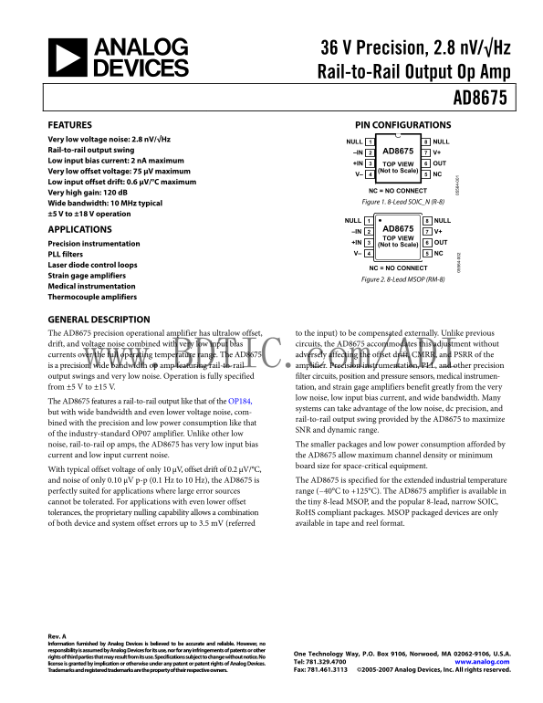
Page 1 Text Content
36 V Precision, 2.8 n V/√Hz Rail-to-Rail Output Op Amp
AD8675 FEATURES PIN CONFIGURATIONS Very low voltage noise: 2.8 n V/√Hz
NULL NULL8
Rail-to-rail output swing AD8675
–IN V+7
Low input bias current: 2 n A maximum
+IN TOP VIEW OUT6 Very low offset voltage: 75 μV maximum (Not to Scale) V– NC5
Low input offset drift: 0.6 μV/°C maximum
NC = NO CONNECT
Very high gain: 120 d B
Wide bandwidth: 10 MHz typical Figure 1. 8-Lead SOIC_N (R-8)
±5 V to ±18 V operation
NULL NULL8
APPLICATIONS AD8675 –IN V+7 TOP VIEW
Precision instrumentation +IN OUT6 (Not to Scale) PLL filters V– NC5
Laser diode control loops
NC = NO CONNECT
Strain gage amplifiers
Figure 2. 8-Lead MSOP (RM-8)
Medical instrumentation Thermocouple amplifiers
GENERAL DESCRIPTION
The AD8675 precision operational amplifier has ultralow offset, to the input) to be compensated externally. Unlike previous drift, and voltage noise combined with very low input bias circuits, the AD8675 accommodates this adjustment without currents over the full operating temperature range. The AD8675 adversely affecting the offset drift, CMRR, and PSRR of the is a precision, wide bandwidth op amp featuring rail-to-rail ww .BDTIC.com/ADI amplifier. Precision instrumentation, PLL, and other precision output swings and very low noise. Operation is fully specified filter circuits, position and pressure sensors, medical instrumen-
from ±5 V to ±15 V. tation, and strain gage amplifiers benefit greatly from the very
low noise, low input bias current, and wide bandwidth. Many
The AD8675 features a rail-to-rail output like that of the OP184,
systems can take advantage of the low noise, dc precision, and
but with wide bandwidth and even lower voltage noise, com-
rail-to-rail output swing provided by the AD8675 to maximize
bined with the precision and low power consumption like that
SNR and dynamic range.
of the industry-standard OP07 amplifier. Unlike other low noise, rail-to-rail op amps, the AD8675 has very low input bias The smaller packages and low power consumption afforded by current and low input current noise. the AD8675 allow maximum channel density or minimum 4-
board size for space-critical equipment.
With typical offset voltage of only 10 μV, offset drift of 0.2 μV/°C, and noise of only 0.10 μV p-p (0.1 Hz to 10 Hz), the AD8675 is The AD8675 is specified for the extended industrial temperature perfectly suited for applications where large error sources range (−40°C to +125°C). The AD8675 amplifier is available in cannot be tolerated. For applications with even lower offset the tiny 8-lead MSOP, and the popular 8-lead, narrow SOIC, tolerances, the proprietary nulling capability allows a combination Ro HS compliant packages. MSOP packaged devices are only
of both device and system offset errors up to 3.5 m V (referred available in tape and reel format.
Rev. A Information furnished by Analog Devices is believed to be accurate and reliable. However, no responsibility is assumed by Analog Devices for its use, nor for any infringements of patents or other
One Technology Way, P.O. Box 9106, Norwood, MA 02062-9106, U.S.A.
rights of third parties that may result from its use. Specifications subject to change without notice. No
license is granted by implication or otherwise under any patent or patent rights of Analog Devices. Tel: 781.329.4700 www.analog.com Trademarks and registered trademarks are the property of their respective owners. Fax: 781.461.3113 ©2005-2007 Analog Devices, Inc. All rights reserved.
Page Summary Contents For AD8675 Analog Devices Data Handbook and Specifications manual
Manual Details
| Brand | Analog Devices |
|---|---|
| Pages | 12 |
| File Size | 350.46 KB |
| Published | June 15, 2026 |
Enter the captcha to get the download link:

Frequently Asked Questions
What is the maximum operating temperature range for the AD8675?
It is specified for the extended industrial temperature range of -40°C to +125°C.
How does the low offset voltage benefit applications like medical instrumentation?
Low offset and drift combined with low noise are perfect for signal integrity in precision sensing (e.g., strain gage amplifiers).
What features make the AD8675 suitable for high-performance measurements?
It offers rail-to-rail output, very low voltage noise (2.8 nV/√Hz), and wide bandwidth up to 10 MHz typically.
Which packages are available for ordering the AD8675 amplifier?
The device is available in 8-Lead Mini Small Outline Package [MSOP] or 8-Lead Standard Small Outline Package [SOIC_N].