AD8397 Analog Devices Data Handbook & Specifications
Summary
The AD8397 is a high-performance, dual voltage operational amplifier featuring rail-to-rail output and exceptional linearity for demanding heavy-load applications. With low noise, 310 mA peak current capability, and a wide 69 MHz bandwidth, it excels in signal amplification where large swings are critical. This manual provides comprehensive technical data covering the pin configuration, electrical characteristics (including stability and bandwidth), thermal guidelines, and best practices for usage in professional audio systems and general AC line driving circuits.
Page 1 Text Content
Rail-to-Rail, High Output Current Amplifier
AD8397 FEATURES PIN CONFIGURATION Dual operational amplifier OUT1 +VS
Voltage feedback –IN1 OUT2 +IN1 –IN2
Wide supply range from 3 V to 24 V
–VS +IN2
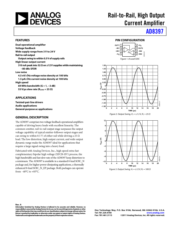
Rail-to-rail output Output swing to within 0.5 V of supply rails Figure 1. 8-Lead SOIC High linear output current
310 m A peak into 32 Ω on ±12 V supplies while maintaining 1.50 −80 d Bc SFDR 1.25 Low noise 1.00 4.5 n V/√Hz voltage noise density at 100 k Hz 0.75 1.5 p A/√Hz current noise density at 100 k Hz 0.50 High speed 0.25
69 MHz bandwidth (G = 1, −3 d B)
53 V/μs slew rate (RLOAD = 25 Ω) –0.25 –0.50 –0.75
APPLICATIONS
Twisted-pair line drivers –1.25 Audio applications –1.50 General-purpose ac applications
TIME (µs)
Figure 2. Output Swing, VS = ±1.5 V, RL = 25 Ω
GENERAL DESCRIPTION The AD8397 comprises two voltage feedback operational amplifiers capable of driving heavy loads with excellent linearity. The common-emitter, rail-to-rail output stage surpasses the output voltage capability of typical emitter-follower output stages and can swing to within 0.5 V of either rail while driving a 25 Ω load. The low distortion, high output current, and wide output dynamic range make the AD8397 ideal for applications that
require a large signal swing into a heavy load. –3
Fabricated with Analog Devices, Inc., high speed extra fast –6 complementary bipolar high voltage (XFCB-HV) process, the
high bandwidth and fast slew rate of the AD8397 keep distortion to
a minimum. The AD8397 is available in a standard 8-lead SOIC_N –12 package and, for higher power dissipating applications, a thermally
TIME (µs)
enhanced 8-lead SOIC_N_EP package. Both packages can operate
Figure 3. Output Swing, VS = ±12 V, RL = 100 Ω
from −40°C to +85°C.
Rev. A Information furnished by Analog Devices is believed to be accurate and reliable. However, no responsibility is assumed by Analog Devices for its use, nor for any infringements of patents or other
One Technology Way, P.O. Box 9106, Norwood, MA 02062-9106, U.S.A.
rights of third parties that may result from its use. Specifications subject to change without notice. No
license is granted by implication or otherwise under any patent or patent rights of Analog Devices. Tel: 781.329.4700 www.analog.com Trademarks and registered trademarks are the property of their respective owners. Fax: 781.461.3113 ©2011 Analog Devices, Inc. All rights reserved.
Page Summary Contents For AD8397 Analog Devices Data Handbook & Specifications
Manual Details
| Brand | Analog Devices |
|---|---|
| Pages | 16 |
| File Size | 239.77 KB |
| Published | June 16, 2026 |
Enter the captcha to get the download link:

Frequently Asked Questions
What is the primary benefit of this amplifier's output stage?
The rail-to-rail output stage allows the output signal to swing within 0.5 V of either supply rail, even when driving heavy loads.
How high is the peak output current it can handle?
It offers a high linear output current capability of 310 mA peak into a 32 Ω load using ±12 V supplies.
What are the temperature and voltage requirements for use?
The device operates from -40°C to +85°C, supporting a wide supply range from 3 V up to 24 V.
Is this amplifier suitable for various types of signals?
Yes; it is ideal for general-purpose AC applications, audio use, and twisted-pair line drivers.