AD7720 Analog Devices Data Handbook & Specifications Manual
Summary
This high-performance 7th order sigma-delta modulator converts continuous analog signals into a high-speed, single-bit digital stream with excellent dynamic range and accuracy. Operating from a +5V supply, it accepts differential inputs and eliminates the need for external sample and hold circuitry. This manual provides comprehensive specifications for system integration, covering detailed static performance metrics, challenging dynamic measurements (like SNR and THD), and crucial guidelines on proper grounding, layout, and power decoupling for optimal high-resolution signal conversion in professional digital systems.
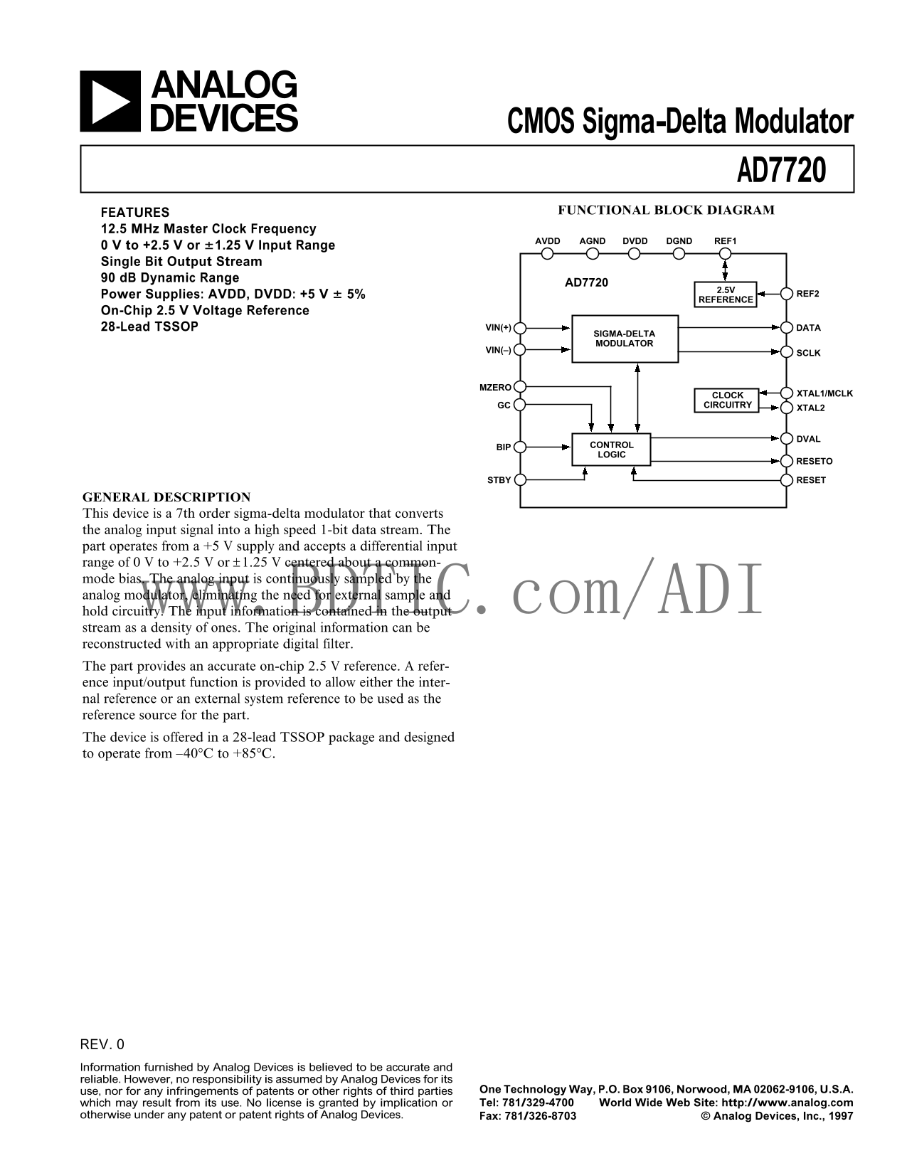
Page 1 Text Content
CMOS Sigma-Delta Modulator
AD7720
FUNCTIONAL BLOCK DIAGRAMFEATURES
12.5 MHz Master Clock Frequency
AVDD AGND DVDD DGND REF1
0 V to +2.5 V or 61.25 V Input Range Single Bit Output Stream 90 d B Dynamic Range
AD7720
Power Supplies: AVDD, DVDD: +5 V 6 5% REF2
REFERENCE
On-Chip 2.5 V Voltage Reference
28-Lead TSSOP VIN(+) DATA
SIGMA-DELTA MODULATOR
VIN(–) SCLK
MZERO
CLOCK XTAL1/MCLK
GC CIRCUITRY
XTAL2
BIP CONTROL LOGIC
RESETO
STBY RESET
GENERAL DESCRIPTION This device is a 7th order sigma-delta modulator that converts the analog input signal into a high speed 1-bit data stream. The part operates from a +5 V supply and accepts a differential input range of 0 V to +2.5 V or ±1.25 V centered about a common- mode bias. The analog input is continuously sampled by the analog modulator, eliminating the need for external sample and
hold circuitry. The input information is contained in the output www.BDTIC.com/ADI stream as a density of ones. The original information can be reconstructed with an appropriate digital filter. The part provides an accurate on-chip 2.5 V reference. A refer- ence input/output function is provided to allow either the inter- nal reference or an external system reference to be used as the reference source for the part. The device is offered in a 28-lead TSSOP package and designed to operate from –40°C to +85°C.
REV. Information furnished by Analog Devices is believed to be accurate and reliable. However, no responsibility is assumed by Analog Devices for its
use, nor for any infringements of patents or other rights of third parties One Technology Way, P.O. Box 9106, Norwood, MA 02062-9106, U.S.A. which may result from its use. No license is granted by implication or Tel: 781/329-4700 World Wide Web Site: http://www.analog.com
otherwise under any patent or patent rights of Analog Devices. Fax: 781/326-8703 © Analog Devices, Inc., 1997
Page Summary Contents For AD7720 Analog Devices Data Handbook & Specifications Manual
Manual Details
| Brand | Analog Devices |
|---|---|
| Pages | 16 |
| File Size | 174.21 KB |
| Published | July 16, 2026 |
Enter the captcha to get the download link:

Frequently Asked Questions
What decoupling capacitors should be used to ensure stable operation?
Use 100 nF ceramic capacitors in DVAL parallel with 10 μF tantalum capacitors, placed ideally right up against the device.
How can I prevent instability when using this high-order sigma-delta modulator?
The system’s AVDD supply should be used and must have a bandwidth that exceeds full scale by 20%.
What is the nominal resolution and dynamic range of the AD7720?
When tested with an Ideal FIR Filter, the device achieves 16 Bits of Resolution and offers a typical Dynamic Range of 90 dB.
What is the input voltage range difference between Bipolar and Unipolar modes?
In Bipolar Mode, the differential input span is ±V /2 V max; in Unipolar Mode, the input range is from 0 to V.