# A B C D E F G H I J K L M N O P Q R S T U V W X Y Z

ADG5412 Analog Devices User's Manual and Specifications

Summary

These quad SPST switches provide reliable, high-voltage latch-up immunity across diverse operating conditions, supporting dual and single supply operation up to 40V. This technical manual is an essential resource for electrical engineers and designers working in demanding fields such as avionics, audio/video switching, data acquisition, and industrial instrumentation. It details comprehensive specifications, functional block diagrams, performance characteristics, and guaranteed low on-resistance switching action for critical power management applications.
📄 Preview 📖 Table of Contents Contents PAGE OF 20

Page 1 Text Content

High Voltage Latch-Up Proof, Quad SPST Switches

ADG5412/ADG5413 FEATURES FUNCTIONAL BLOCK DIAGRAMS Latch-up proof

8 k V human body model (HBM) ESD rating

IN1 IN1

Low on resistance (<10 Ω) D1 D1 ±9 V to ±22 V dual-supply operation

9 V to 40 V single-supply operation

IN2 IN2

48 V supply maximum ratings

Fully specified at ±15 V, ±20 V, +12 V, and +36 V ADG5412 ADG5413

VSS to VDD analog signal range

IN3 IN3

APPLICATIONS D3 D3

Relay replacement S4 S4

Automatic test equipment IN4 IN4

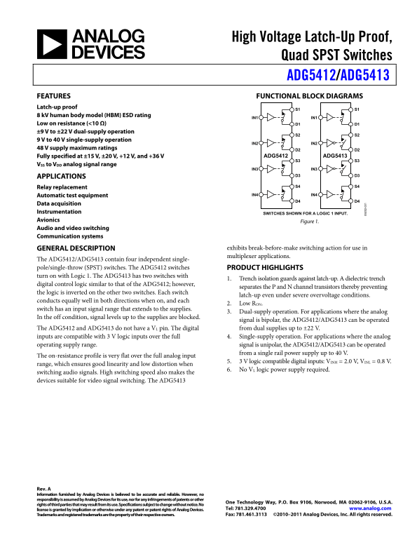
Data acquisition Instrumentation SWITCHES SHOWN FOR A LOGIC 1 INPUT. Avionics Figure 1. Audio and video switching Communication systems

GENERAL DESCRIPTION exhibits break-before-make switching action for use in multiplexer applications.

The ADG5412/ADG5413 contain four independent single- pole/single-throw (SPST) switches. The ADG5412 switches PRODUCT HIGHLIGHTS turn on with Logic 1. The ADG5413 has two switches with

1. Trench isolation guards against latch-up. A dielectric trench

digital control logic similar to that of the ADG5412; however,

separates the P and N channel transistors thereby preventing

the logic is inverted on the other two switches. Each switch

latch-up even under severe overvoltage conditions.

conducts equally well in both directions when on, and each

2. Low RON.

switch has an input signal range that extends to the supplies.

3. Dual-supply operation. For applications where the analog

In the off condition, signal levels up to the supplies are blocked.

signal is bipolar, the ADG5412/ADG5413 can be operated

The ADG5412 and ADG5413 do not have a VL pin. The digital from dual supplies up to ±22 V.

inputs are compatible with 3 V logic inputs over the full 4. Single-supply operation. For applications where the analog

operating supply range. signal is unipolar, the ADG5412/ADG5413 can be operated

from a single rail power supply up to 40 V.

The on-resistance profile is very flat over the full analog input

5. 3 V logic compatible digital inputs: VINH = 2.0 V, VINL = 0.8 V.

range, which ensures good linearity and low distortion when 2-

6. No VL logic power supply required.

switching audio signals. High switching speed also makes the devices suitable for video signal switching. The ADG5413

Rev. A Information furnished by Analog Devices is believed to be accurate and reliable. However, no responsibility is assumed by Analog Devices for its use, nor for any infringements of patents or other

One Technology Way, P.O. Box 9106, Norwood, MA 02062-9106, U.S.A.

rights of third parties that may result from its use. Specifications subject to change without notice. No

license is granted by implication or otherwise under any patent or patent rights of Analog Devices. Tel: 781.329.4700 www.analog.com Trademarks and registered trademarks are the property of their respective owners. Fax: 781.461.3113 ©2010–2011 Analog Devices, Inc. All rights reserved.

Page Summary Contents For ADG5412 Analog Devices User's Manual and Specifications

Page 1 High Voltage Latch-Up Proof, Quad SPST Switches ADG5412/ADG5413 FEATURES FUNCTIONAL BLOCK DIAGRAMS Latch-up proof 8 k V human body model (HBM) ESD rating IN1 IN1 Low on resistance (&lt;10 Ω) D1 D1 ±9 ...
Page 2 ADG5412/ADG5413 TABLE OF CONTENTS Features Continuous Current per Channel, Sx or Dx..............................7 Applications............................................................................
Page 3 ADG5412/ADG5413 SPECIFICATIONS ±15 V DUAL SUPPLY VDD = +15 V ± 10%, VSS = −15 V ± 10%, GND = 0 V, unless otherwise noted. Table 1. Parameter 25°C −40°C to +85°C −40°C to +125°C Unit Test Conditions/Co...
Page 4 ADG5412/ADG5413 Parameter 25°C −40°C to +85°C −40°C to +125°C Unit Test Conditions/Comments POWER REQUIREMENTS VDD = +16.5 V, VSS = −16.5 V IDD 45 μA typ Digital inputs = 0 V or VDD 55 70 μA max ISS 0...
Page 5 ADG5412/ADG5413 Parameter 25°C −40°C to +85°C −40°C to +125°C Unit Test Conditions/Comments Total Harmonic Distortion + Noise 0.007 % typ RL = 1 kΩ, 20 V p-p, f = 20 Hz to 20 k Hz; see Figure 28 −3 d ...
Page 6 ADG5412/ADG5413 Parameter 25°C −40°C to +85°C −40°C to +125°C Unit Test Conditions/Comments Break-Before-Make Time Delay, t D 70 ns typ RL = 300 Ω, CL = 35 p F (ADG5413 Only) 38 ns min VS1 = VS2 = 8 V...
Page 7 ADG5412/ADG5413 Parameter 25°C −40°C to +85°C −40°C to +125°C Unit Test Conditions/Comments DIGITAL INPUTS Input High Voltage, VINH 2.0 V min Input Low Voltage, VINL 0.8 V max Input Current, IINL or I...
Page 8 ADG5412/ADG5413 ABSOLUTE MAXIMUM RATINGS TA = 25°C, unless otherwise noted. Table 6. Stresses above those listed under Absolute Maximum Ratings Parameter Rating may cause permanent damage to the devic...
Page 9 ADG5412/ADG5413 PIN CONFIGURATIONS AND FUNCTION DESCRIPTIONS IN1 IN216 S1 S214 PIN 1 ADG5412/ INDICATOR VSS ADG5413 VDD13 2VSS ADG5412/ VDD GND TOP VIEW NC12 3GND ADG5413 NC (Not to Scale) S4 S311 TOP...
Page 10 ADG5412/ADG5413 ES IS TA (Ω ES IS TA (Ω ES IS TA (Ω TYPICAL PERFORMANCE CHARACTERISTICS TA = 25°C VDD = +10V TA = 25°C VDD = +9V VSS = –10V VSS = –9V VDD = 32.4V VSS = 0V VDD = +11V VDD = 36V VSS = –1...
Page 11 ADG5412/ADG5413 LE EN (n ES IS TA (Ω ES IS TA (Ω VDD = 12V VDD = +20V VSS = 0V VSS = –20V VBIAS = +15V/–15V ID, IS (ON) + + 0.6 ID, IS (ON) – – TA = +125°C 0.4 IS (OFF) + – TA = +85°C 0.2 ID (OFF) – +...
Page 12 ADG5412/ADG5413 IN JE TI (p SS TA LK (d FF IS LA TI (d TA = 25°C TA = 25°C VDD = +15V VDD = +15V –10 –10 VSS = –15V VSS = –15V NO DECOUPLING CAPACITORS –70 –70 DECOUPLING CAPACITORS FREQUENCY (Hz) FRE...
Page 13 ADG5412/ADG5413 TI (n s) t ON (12V) t ON (±20V) t ON (±15V) t OFF (±15V) t ON (36V) t OFF (12V) t OFF (36V) t OFF (±20V) TEMPERATURE (°C) Figure 22. t ON, t OFF Times vs. Temperature Rev. A | Page 13 ...
Page 14 ADG5412/ADG5413 TEST CIRCUITS IS (OFF) ID (OFF) Sx Dx ID (ON) Sx Dx VS VD VS VD Figure 23. On Leakage Figure 27. Off Leakage VDD VSS 0.1µF 0.1µF AUDIO PRECISION VDD VSS IDS 2- INx VS 2- Dx VIN RL Sx D...
Page 15 ADG5412/ADG5413 VDD VSS 0.1µF 0.1µF VIN 50% 50% 0V VDD VSS 90%90% S1 D1 VOUT1 VS1 VOUT1 0V RL CL VS2 VOUT2 300Ω 35p F RL CL 300Ω 35p F VOUT2 IN1, ADG5413 0V IN2 GND Figure 30. Break-Before-Make Time D...
Page 16 ADG5412/ADG5413 TERMINOLOGY IDD CIN IDD represents the positive supply current. CIN is the digital input capacitance. ISS t ON ISS represents the negative supply current. t ON represents the delay bet...
Page 17 ADG5412/ADG5413 TRENCH ISOLATION NMOS PMOS In the ADG5412 and ADG5413, an insulating oxide layer (trench) is placed between the NMOS and the PMOS transistors of each CMOS switch. Parasitic junctions, ...
Page 18 ADG5412/ADG5413 APPLICATIONS INFORMATION The ADG54xx family of switches and multiplexers provide a allow single-supply operation from 9 V to 40 V and dual-supply robust solution for instrumentation, i...
Page 19 ADG5412/ADG5413 OUTLINE DIMENSIONS 4.40 BSC 4.30 PIN 1 1.20 MAX 0.19 SEATING PLANE COPLANARITY 0.10 COMPLIANT TO JEDEC STANDARDS MO-153-AB Figure 34. 16-Lead Thin Shrink Small Outline Package [TSSOP] ...
Page 20 ADG5412/ADG5413 NOTES ©2010–2011 Analog Devices, Inc. All rights reserved. Trademarks and registered trademarks are the property of their respective owners. D09202-0-6/11(A) Rev. A | Page 20 of 20

Manual Details

Brand Analog Devices
Pages 20
File Size 334.30 KB
Published May 14, 2026
123 views

Enter the captcha to get the download link:

captcha

Frequently Asked Questions

How is this switch protected against overvoltage?

It features trench isolation guards that prevent latch-up even under severe overvoltage or high voltage conditions.

Can the ADG5412/ADG5413 operate with a single or dual power supply?

Yes, it supports both dual-supply operation (±9 V to ±22 V) and single-supply operation up to 40 V.

What type of logic signals can the device easily interface with?

The switches are compatible with 3V logic inputs and turn on using a Logic 1 input signal.