# A B C D E F G H I J K L M N O P Q R S T U V W X Y Z

AD5378 Analog Devices User's Manual and Specifications

Summary

This high-precision AD5378 DAC offers 32 channels of 14-bit bipolar voltage output, featuring both parallel and serial interfaces in a compact CSPBGA package. This manual provides comprehensive technical details, covering advanced aspects like timing characteristics, power-on reset sequences, signal decoding, and multiple operational modes (e.g., daisy-chaining). It is engineered for demanding industrial applications, including automatic test equipment (ATE), variable optical attenuators, and complex control systems requiring stable, high-accuracy analog signal generation.
📄 Preview 📖 Table of Contents Contents PAGE OF 28

Page 1 Text Content

32-Channel, 14-Bit, Parallel and Serial Input, Bipolar Voltage Output DAC

AD5378

IN TE FA

FEATURES Interface options

ST TE IN Parallel interface

32-channel DAC in 13 mm × 13 mm 108-lead CSPBGA

DSP/microcontroller-compatible 3-wire serial interface

Guaranteed monotonic to 14 bits

2.5 V to 5.5 V JEDEC-compliant digital levels

Buffered voltage outputs

SDO daisy-chaining option

Output voltage span of 3.5 V × VREF(+)

Power-on reset

Maximum output voltage span of 17.5 V

Digital reset (RESET pin and soft reset function)

System calibration function allowing user-programmable offset and gain Pseudo differential outputs relative to REFGND APPLICATIONS Clear function to user-defined REFGND (CLR pin) Level setting in automatic test equipment (ATE)

Simultaneous update of DAC outputs (LDAC pin) Variable optical attenuators (VOAs) DAC increment/decrement mode Optical switches Channel grouping and addressing features Industrial control systems

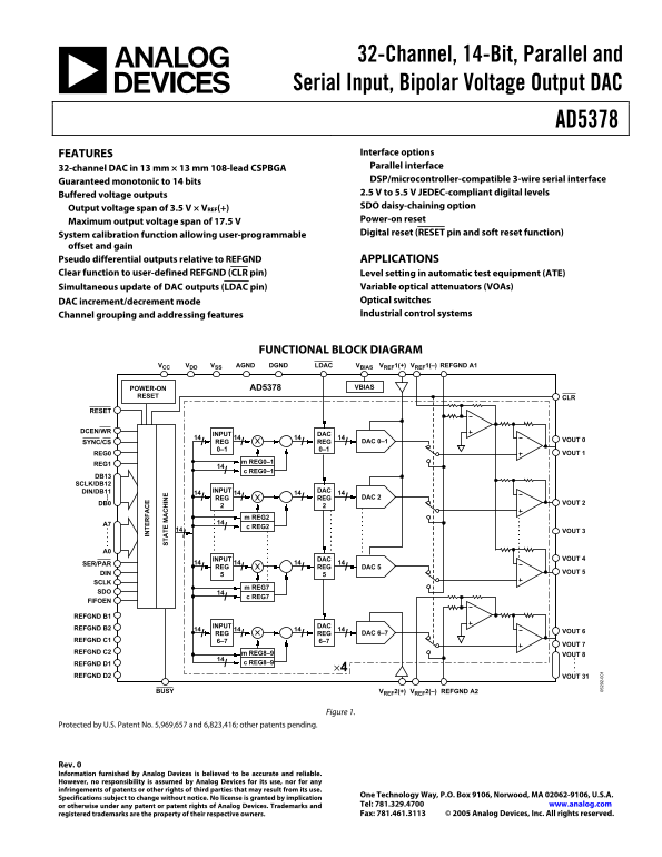
FUNCTIONAL BLOCK DIAGRAM

VCC VDD VSS AGND DGND LDAC VBIAS VREF1(+) VREF1(–) REFGND A1

POWER-ON AD5378 VBIAS

RESET CLR

RESET

DCEN/WR

INPUT DAC 14/ 14/ 14/ 14/

REG REG DAC 0–1 VOUT 0

SYNC/CS

REG0 VOUT 1

m REG0–1

c REG0–1

DB13 SCLK/DB12

DIN/DB11 INPUT DAC 14/ 14/ 14/ 14/

REG REG DAC 2

DB0 VOUT 2

m REG2

c REG2

14/ VOUT 3

INPUT DAC VOUT 4

SER/PAR 14/ 14/ 14/ 14/ REG REG DAC 5

DIN VOUT 5

m REG7

SDO 14/

c REG7

FIFOEN 2-

REFGND B1

INPUT DAC

REFGND B2 14/ 14/ 14/ 14/

DAC 6–7 VOUT 6

REG REG

REFGND C1 6–7 6–7

VOUT 7

REFGND C2 m REG8–9

VOUT 8

REFGND D1 c REG8–9

REFGND D2 VOUT 31

BUSY VREF2(+) VREF2(–) REFGND A2

Figure 1.

Protected by U.S. Patent No. 5,969,657 and 6,823,416; other patents pending.

Rev. 0 Information furnished by Analog Devices is believed to be accurate and reliable. However, no responsibility is assumed by Analog Devices for its use, nor for any infringements of patents or other rights of third parties that may result from its use.

One Technology Way, P.O. Box 9106, Norwood, MA 02062-9106, U.S.A.

Specifications subject to change without notice. No license is granted by implication

or otherwise under any patent or patent rights of Analog Devices. Trademarks and Tel: 781.329.4700 www.analog.com registered trademarks are the property of their respective owners. Fax: 781.461.3113 © 2005 Analog Devices, Inc. All rights reserved.

Page Summary Contents For AD5378 Analog Devices User's Manual and Specifications

Page 1 32-Channel, 14-Bit, Parallel and Serial Input, Bipolar Voltage Output DAC AD5378 IN TE FA FEATURES Interface options ST TE IN Parallel interface 32-channel DAC in 13 mm × 13 mm 108-lead CSPBGA DSP/mic...
Page 2 AD5378 TABLE OF CONTENTS General Description ..........................................................................3 Clear Function Specifications.....................................................
Page 3 AD5378 GENERAL DESCRIPTION The AD5378 contains 32 14-bit DACs in one CSPBGA package. The DAC outputs are updated when the DAC registers receive The AD5378 provides a bipolar output range determined by...
Page 4 AD5378 SPECIFICATIONS VCC = 2.7 V to 5.5 V; VDD = 11.4 V to 16.5 V; VSS = −11.4 V to −16.5 V; VREF(+) = +5 V; VREF(−) = −3.5 V; AGND = DGND = REFGND = 0 V; VBIAS = 5 V; CL = 200 p F to GND; RL = 11 kΩ...
Page 5 AD5378 Parameter A Version1 Unit Test Conditions/Comments POWER REQUIREMENTS VCC 2.7/5.5 V min/max VDD 8.5/16.5 V min/max VSS −3/−16.5 V min/max Power Supply Sensitivity2 ∆ Full Scale/∆ VDD −75 d B ty...
Page 6 AD5378 TIMING CHARACTERISTICS SERIAL INTERFACE VCC = 2.7 V to 5.5 V; VDD = 11.4 V to 16.5 V; VSS = −11.4 V to −16.5 V; VREF(+) = +5 V; VREF(−) = −3.5 V; AGND = DGND = REFGND = 0 V; VBIAS = 5 V, FIFOEN...
Page 7 AD5378 DIN DB23 DB0 LDAC1 VOUT1 LDAC2 VOUT2 1LDAC ACTIVE DURING BUSY. 2LDAC ACTIVE AFTER BUSY. RESET VOUT t19 Figure 4. Serial Interface Timing Diagram (Standalone Mode) Rev. 0 | Page 7 of 28
Page 8 AD5378 DIN D0 D0'D23'D23 INPUT WORD FOR DAC N INPUT WORD FOR DAC N+1 SDO D23 D0 INPUT WORD FOR DAC NUNDEFINED Figure 5. Serial Interface Timing Diagram (Daisy-Chain Mode) Rev. 0 | Page 8 of 28
Page 9 AD5378 PARALLEL INTERFACE VCC = 2.7 V to 5.5 V; VDD = 11.4 V to 16.5 V; VSS = −11.4 V to −16.5 V; AGND = DGND = DUTGND = 0 V; VREF(+) = +5 V; VREF(−) = −3.5 V, FIFOEN = 0 V; all specifications TMIN to...
Page 10 AD5378 REG0, REG1, A7–A02 DB12–DB0 LDAC1 VOUT1 LDAC2 VOUT2 1LDAC ACTIVE DURING BUSY. 2LDAC ACTIVE AFTER BUSY. RESET VOUT t21 Figure 6. Parallel Interface Timing Diagram Rev. 0 | Page 10 of 28
Page 11 AD5378 ABSOLUTE MAXIMUM RATINGS TA = 25°C, unless otherwise noted. Transient currents of up to 100 m A do not cause SCR latch-up. Table 7. Stresses above those listed under Absolute Maximum Ratings Pa...
Page 12 AD5378 PIN CONFIGURATION AND FUNCTION DESCRIPTIONS AD5378 TOP VIEW Figure 7. Pin Configuration Table 8. 108-Lead CSPBGA Ball Configuration CSPBGA No. Ball Name CSPBGA No. Ball Name CSPBGA No. Ball Nam...
Page 13 AD5378 Table 9. Pin Function Descriptions Pin Description VCC(1–3) Logic Power Supply. 2.7 V to 5.5 V. These pins should be decoupled with 0.1 µF ceramic capacitors and 10 µF tantalum capacitors. VSS(...
Page 14 AD5378 Pin Description FIFOEN FIFO Enable. Level sensitive, active high. When connected to DVDD, the internal FIFO is enabled, allowing the user to write to the device at full speed. FIFO is available...
Page 15 AD5378 IN ER (L SB FR EQ EN IN (L SB s) TYPICAL PERFORMANCE CHARACTERISTICS 1.5 VDD = +12V VSS = –12V VREF(+) = +5V VREF(–) = –3.5V TMAX = 85°C 0.5 FS VDD = +12V VSS = –12V VREF(+) = +5V –3 VREF(–) = ...
Page 16 PL IT (V PL IT (V (m AD5378 3.5 VDD = +12V TA = 25°C VSS = –12V VDD = +12V 3.0 VREF(+) = +5V VSS = –12V VREF(–) = –3.5V VREF(+) = +5V VREF(–) = –3.5V SUPPLY VOLTAGE (V) Figure 14. ICC vs. Supply Figur...
Page 17 AD5378 TERMINOLOGY Relative Accuracy DC Crosstalk Relative accuracy or endpoint linearity is a measurement of the The 32 DAC outputs are buffered by op amps that share maximum deviation from a straigh...
Page 18 AD5378 FUNCTIONAL DESCRIPTION DAC ARCHITECTURE—GENERAL Figure 19 shows a single DAC channel and its associated registers. The power-on values for the m and c registers are full The AD5378 contains 32 ...
Page 19 AD5378 VBIAS FUNCTION If this offset error too large to calibrated out, it is possible to adjust the negative reference value to account for this by using The AD5378 on-chip voltage generator provides...
Page 20 AD5378 Software Clear CALIBRATION Loading a clear code to the x1 registers also enables the user to The user can perform a system calibration by overwriting the set VOUT0 to VOUT31 to the REFGND level...
Page 21 AD5378 the parallel interface is disabled, so it is not possible to write to FIFO VS. NON-FIFO OPERATION the part. Any transitions on LDAC during the power-on period Data can be loaded to the AD5378 r...
Page 22 AD5378 INTERFACES A7 to A0 Pins The AD5378 contains parallel and serial interfaces. The active interface is selected via the SER/PAR pin. Each of the 32 DAC channels can be addressed individually. In ...
Page 23 AD5378 Daisy-Chain Mode clock cycles must equal 24N, where N is the total number of AD5378 devices in the chain. If fewer than 24 clocks are For systems that contain several DACs, the SDO pin can be a...
Page 24 AD5378 DATA DECODING Table 15. Gain Data Format (REG1 = 0, REG0 = 1) The AD5378 contains a 14-bit data bus, DB13 to DB0. Depend- DB12 to DB1 Gain ing on the value of REG1 and REG0, this data is loaded...
Page 25 AD5378 ADDRESS DECODING The AD5378 contains an 8-bit address bus, A7 to A0. This The REG1 and REG0 bits in the special function register (SFR) address bus allows each DAC input register (x1), each off...
Page 26 AD5378 POWER SUPPLY DECOUPLING and reduce the effects of glitches on the power supply line. Fast In any circuit where accuracy is important, careful considera- switching digital signals should be shie...
Page 27 AD5378 TYPICAL APPLICATION CIRCUIT The high channel count of the AD5378 makes it wellsuited to In addition to the DAC levels required in the ATE system applications requiring high levels of integratio...
Page 28 AD5378 OUTLINE DIMENSIONS A1 CORNER INDEX AREA 13.00 BSC SQ BALL A1 INDICATOR 11.00 TOP VIEW BSC SQ 1.00 BSC *1.85 DETAIL A 1.55 DETAIL A 1.05 1.00 0.90 0.12 MAX SEATING COPLANARITY *0.64 TYP PLANE BA...