# A B C D E F G H I J K L M N O P Q R S T U V W X Y Z

ANALOG DEVICES ADN2806 User's Guide

Summary

The ADN2806 is a specialized Clock and Data Recovery IC for handling 622 Mbps NRZ data, designed to exceed strict SONET jitter requirements. This chip provides automatic, reference clock-free locking for high-speed optical receivers. The manual offers comprehensive technical support covering the device's theory of operation, detailed jitter specifications, functional block diagrams, electrical characteristics (including power and thermal details), and critical PCB design guidelines. It is essential reading for engineers integrating highly reliable, low-power BPON ONT and WDM transponder systems.
📄 Preview 📖 Table of Contents Contents PAGE OF 20

Page 1 Text Content

622 Mbps Clock and Data Recovery IC

Data Sheet ADN2806 FEATURES GENERAL DESCRIPTION Exceeds SONET requirements for jitter transfer/

The ADN2806 provides the receiver functions for clock and

generation/tolerance

data recovery, and data retiming for 622 Mbps NRZ data. The

Patented clock recovery architecture

ADN2806 automatically locks to 622 Mbps data without the

No reference clock required

need for an external reference clock or programming. All

Loss-of-lock indicator

SONET jitter requirements are met, including jitter transfer,

I2C® interface to access optional features

jitter generation, and jitter tolerance. All specifications are

Single-supply operation: 3.3 V

quoted for −40°C to +85°C ambient temperature, unless

Low power: 359 m W typical

otherwise noted.

5 mm × 5 mm, 32-lead LFCSP, Pb free

This device, together with a PIN diode, TIA preamplifier, and a

APPLICATIONS

lim amp can implement a highly integrated, low cost, low power

BPON ONT

fiber optic receiver.

SONET OC-12

WDM transponders The ADN2806 is available in a compact 5 mm × 5 mm, Regenerators/repeaters 32-lead LFCSP.

Test equipment Broadband cross-connects and routers

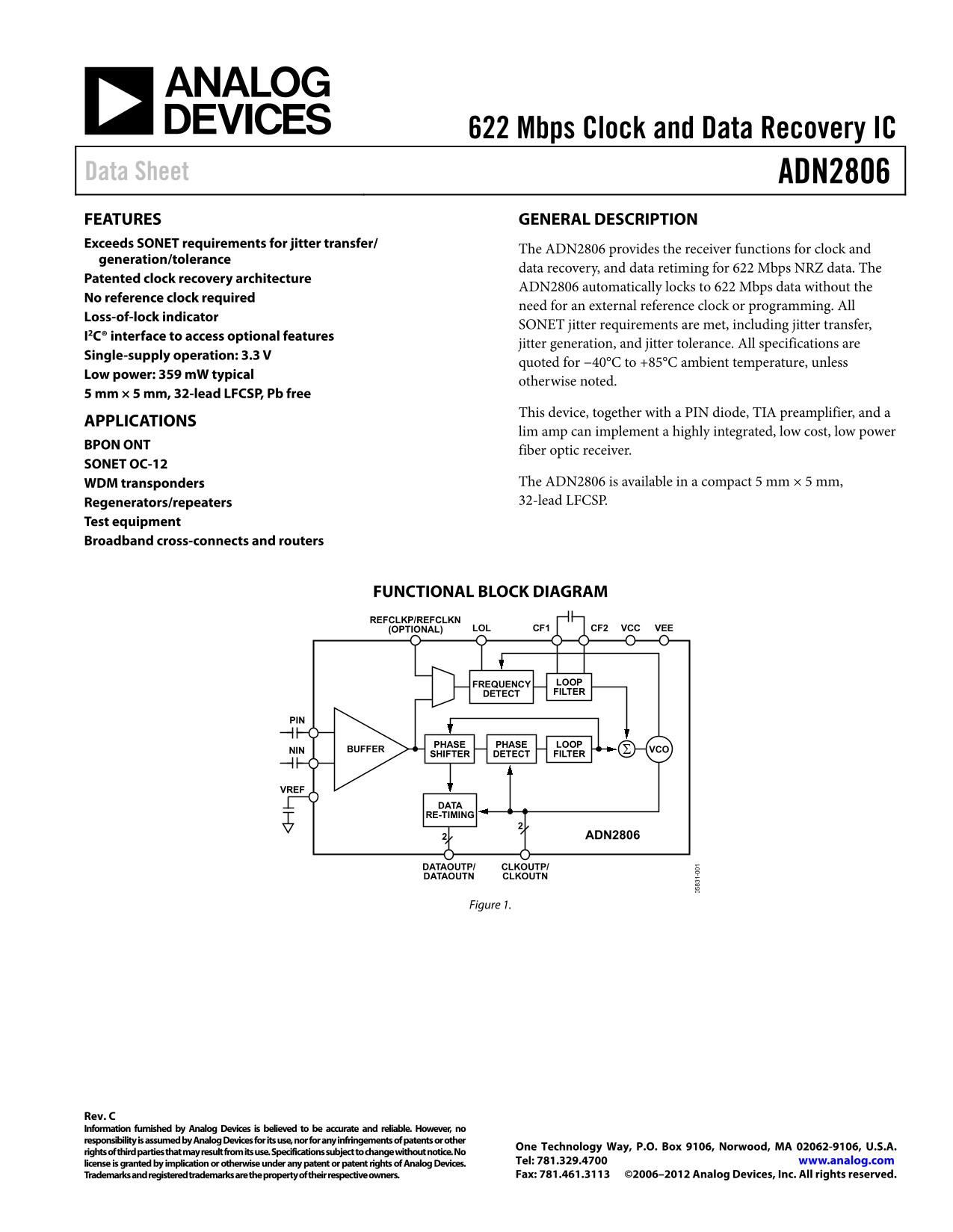
FUNCTIONAL BLOCK DIAGRAM REFCLKP/REFCLKN

(OPTIONAL) LOL CF2 VCC VEECF1

FREQUENCY LOOP DETECT FILTER

PHASE LOOP

NIN BUFFER VCOPHASE

SHIFTER DETECT FILTER

DATA RE-TIMING

ADN2806

DATAOUTP/ CLKOUTP/ DATAOUTN CLKOUTN

Figure 1.

Rev. C Information furnished by Analog Devices is believed to be accurate and reliable. However, no responsibility is assumed by Analog Devices for its use, nor for any infringements of patents or other

One Technology Way, P.O. Box 9106, Norwood, MA 02062-9106, U.S.A.

rights of third parties that may result from its use. Specifications subject to change without notice. No

license is granted by implication or otherwise under any patent or patent rights of Analog Devices. Tel: 781.329.4700 www.analog.com Trademarks and registered trademarks are the property of their respective owners. Fax: 781.461.3113 ©2006–2012 Analog Devices, Inc. All rights reserved.

Page Summary Contents For ANALOG DEVICES ADN2806 User's Guide

Page 1 622 Mbps Clock and Data Recovery IC Data Sheet ADN2806 FEATURES GENERAL DESCRIPTION Exceeds SONET requirements for jitter transfer/ The ADN2806 provides the receiver functions for clock and generation...
Page 2 ADN2806 TABLE OF CONTENTS Features 1  Jitter Specifications......................................................................... 10  Applications......................................................
Page 3 ADN2806 SPECIFICATIONS TA = TMIN to TMAX, VCC = VMIN to VMAX, VEE = 0 V, CF = 0.47 μF, SLICEP = SLICEN = VEE, input data pattern: PRBS 223 − 1, unless otherwise noted. Table 1. Parameter Conditions Mi...
Page 4 ADN2806 OUTPUT AND TIMING SPECIFICATIONS Table 3. Parameter Conditions Min Typ Max Unit LVDS OUTPUT CHARACTERISTICS (CLKOUTP/CLKOUTN, DATAOUTP/DATAOUTN) Output Voltage High VOH (see Figure 3) 1475 m V...
Page 5 ADN2806 ABSOLUTE MAXIMUM RATINGS TA = TMIN to TMAX, VCC = VMIN to VMAX, VEE = 0 V, CF = 0.47 μF, unless otherwise noted. Table 4. Stress above those listed under Absolute Maximum Ratings may Parameter...
Page 6 ADN2806 TIMING CHARACTERISTICS CLKOUTP DATAOUTP/ DATAOUTN Figure 2. Output Timing DIFFERENTIAL CLKOUTP/N, DATAOUTP/N VOS |VOD| Figure 3. Differential Output Specifications RLOAD VDIFF SIMPLIFIED LVDS ...
Page 7 ADN2806 PIN CONFIGURATION AND FUNCTION DESCRIPTIONS 1TEST1 PIN 1 24 VCC VCC INDICATOR 23 VEE VREF 22 NC NIN ADN2806 21 SDA PIN TOP VIEW 20 SCK NC (Not to Scale) 19 SADDR5 NC 18 VCC VEE 17 VEE 1. NC = ...
Page 8 ADN2806 I2C INTERFACE TIMING AND INTERNAL REGISTER DESCRIPTION SLAVE ADDRESS [6...0] CTRL. MSB = 1 SET BY 0 = WR PIN 19 1 = RD Figure 6. Slave Address Configuration SLAVE ADDR, LSB = 0 (WR) A(S) ADDR ...
Page 9 ADN2806 Table 6. Internal Register Map1 Reg Name R/W Addr D7 D6 D5 D4 D3 D2 D1 D0 FREQ0 R 0x0 MSB LSB FREQ1 R 0x1 MSB LSB FREQ2 R 0x2 0 MSB LSB MISC R 0x4 x x LOS Static LOL Data rate x x status LOL s...
Page 10 ADN2806 JITTER SPECIFICATIONS The ADN2806 CDR is designed to achieve the best bit- error-rate (BER) performance and to exceed the jitter transfer, generation, and tolerance specifications proposed for...
Page 11 ADN2806 THEORY OF OPERATION The ADN2806 is a delay- and phase-locked loop circuit for psh clock recovery and data retiming from an NRZ encoded data X(s) e(s)INPUT stream. The phase of the input data s...
Page 12 ADN2806 At medium jitter frequencies, the gain and tuning range of the The gain of the loop integrator is small for high jitter VCO are not large enough to track input jitter. In this case, the freque...
Page 13 ADN2806 FUNCTIONAL DESCRIPTION FREQUENCY ACQUISITION LOL Detector Operation Using a Reference Clock The ADN2806 acquires frequency from the data. The lock In REFCLK mode, a reference clock is used as ...
Page 14 ADN2806 Squelch data outputs or clock outputs mode is selected when The ADN2806 acts as a standard slave device on the bus. The data CTRLC[1] is 1. In this mode, when the SQUELCH input is on the SDA p...
Page 15 ADN2806 REFERENCE CLOCK (OPTIONAL) There are two mutually exclusive uses, or modes, of the reference clock. The reference clock can be used either to help A reference clock is not required to perform ...
Page 16 ADN2806 3. Read back MISC[2]. If it is 0, the measurement is not Using the Reference Clock to Measure Data Frequency complete. If it is 1, the measurement is complete and the The user can also provide...
Page 17 ADN2806 APPLICATIONS INFORMATION PCB DESIGN GUIDELINES If connections to the supply and ground are made through vias, the use of multiple vias in parallel helps to reduce series Proper RF PCB design t...
Page 18 ADN2806 Choosing AC Coupling Capacitors Transmission Lines AC coupling capacitors at the input (PIN, NIN) and output Minimizing reflections in the ADN2806 requires use of 50 Ω (DATAOUTP, DATAOUTN) of ...
Page 19 ADN2806 ADN2806 LIM V1 CIN V2 50Ω DATAOUTP VREF BUFFER CDR CINV1b V2b 50Ω DATAOUTN VDIFF VTH VDIFF = V2–V2b VTH = ADN2806 THRESHOLD NOTES: 1. DURING DATA PATTERNS WITH HIGH TRANSITION DENSITY, DIFFERE...
Page 20 ADN2806 OUTLINE DIMENSIONS 5.10 0.30 5.00 SQ 0.25 4.90 0.18 PIN 1 INDICATOR PIN 1 INDICATOR 0.50 BSC EXPOSED 3.25 3.10 SQ 2.95 0.50 0.25 MIN BOTTOM VIEWTOP VIEW 0.40 0.30 FOR PROPER CONNECTION OF 0.80...

Manual Details

Brand Analog Devices
Pages 20
File Size 313.56 KB
Published July 15, 2026
0 views

Enter the captcha to get the download link:

captcha

Frequently Asked Questions

Does the ADN2806 require an external reference clock?

No, it uses a patented clock recovery architecture and automatically locks to 622 Mbps data without needing an external reference clock or programming.

What is the operating supply voltage and temperature range?

It operates on single-supply operation at 3.3 V from -40°C to +85°C ambient temperature.

What are some typical applications for this IC?

It can implement a highly integrated, low cost, low power BPON ONT fiber optic receiver, and is used in WDM transponders.

What form factor and package type is the ADN2806 available in?

It comes in a compact 5 mm × 5 mm, 32-lead LFCSP package.

Can this chip handle standard SONET jitter requirements?

Yes, it meets all SONET jitter requirements, including monitoring jitter transfer and jitter tolerance.