ADG1211 Low Capacitance, Low Charge Injection, ±15 V +12 V iCMOS™ Quad SPST Switch
Summary
These quad SPST switches are designed using advanced iCMOS technology to deliver high performance with ultralow power consumption (<0.03 μW) and minimal charge injection (<1 pC). Built for demanding applications, they feature 33V supply compatibility while maintaining low capacitance. This manual provides comprehensive details on the ADG1211/ADG1212/ADG1213 series, covering functional block diagrams, dual/single power specifications, and best practices for implementation. Ideal for engineers working on portable, battery-powered systems such as data acquisition (DAQ), automatic test equipment, video routing, and complex communication networks needing stable signal switching.
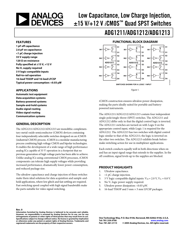
Page 1 Text Content
Low Capacitance, Low Charge Injection, ±15 V/+12 V i CMOS™ Quad SPST Switches
ADG1211/ADG1212/ADG1213
FUNCTIONAL BLOCK DIAGRAM FEATURES
1 p F off capacitance
2.6 p F on capacitance IN1 IN1 IN1
<1 p C charge injection
33 V supply range
IN2 IN2 IN2
120 Ω on resistance D2 D2 D2
ADG1211 ADG1212 ADG1213
Fully specified at ±15 V, +12 V S3 S3 S3
IN3 IN3 IN3
No VL supply required
3 V logic-compatible inputs
Rail-to-rail operation IN4 IN4 IN4
16-lead TSSOP and 16-lead LFCSP Typical power consumption: <0.03 μW
SWITCHES SHOWN FOR A LOGIC 1 INPUT
APPLICATIONS Figure 1. Automatic test equipment Data acquisition systems
Battery-powered systems i CMOS construction ensures ultralow power dissipation, Sample-and-hold systems making the parts ideally suited for portable and battery- powered instruments.
Audio signal routing Video signal routing The ADG1211/ADG1212/ADG1213 contain four independent Communication systems
single-pole/single-throw (SPST) switches. The ADG1211 and ADG1212 differ only in that the digital control logic is inverted.
GENERAL DESCRIPTION
The ADG1211 switches are turned on with Logic 0 on the The ADG1211/ADG1212/ADG1213 are monolithic complemen- appropriate control input, while Logic 1 is required for the tary metal-oxide semiconductor (CMOS) devices containing ADG1212. The ADG1213 has two switches with digital control four independently selectable switches designed on an i CMOS logic similar to that of the ADG1211; the logic is inverted on (industrial CMOS) process. i CMOS is a modular manufacturing the other two switches. The ADG1213 exhibits break-before- process combining high voltage CMOS and bipolar technologies. make switching action for use in multiplexer applications.
It enables the development of a wide range of high performance
Each switch conducts equally well in both directions when on
analog ICs capable of 33 V operation in a footprint that no
and has an input signal range that extends to the supplies. In the
previous generation of high voltage parts has been able to achieve.
off condition, signal levels up to the supplies are blocked.
Unlike analog ICs using conventional CMOS processes, i CMOS components can tolerate high supply voltages while providing increased performance, dramatically lower power consumption,
PRODUCT HIGHLIGHTS
and reduced package size. 8-
1. Ultralow capacitance.
The ultralow capacitance and charge injection of these switches 2. <1 p C charge injection. make them ideal solutions for data acquisition and sample-and- 3. 3 V logic-compatible digital inputs: V IH = 2.0 V, VIL = 0.8 V. hold applications, where low glitch and fast settling are required. 4. No VL logic power supply required. Fast switching speed coupled with high signal bandwidth make 5. Ultralow power dissipation: <0.03 μW. the parts suitable for video signal switching. 6. 16-lead TSSOP and 3 mm × 3 mm LFCSP packages.
Rev. 0 Information furnished by Analog Devices is believed to be accurate and reliable. However, no responsibility is assumed by Analog Devices for its use, nor for any infringements of patents or other rights of third parties that may result from its use.
One Technology Way, P.O. Box 9106, Norwood, MA 02062-9106, U.S.A.
Specifications subject to change without notice. No license is granted by implication
or otherwise under any patent or patent rights of Analog Devices. Trademarks and Tel: 781.329.4700 www.analog.com registered trademarks are the property of their respective owners. Fax: 781.461.3113 © 2005 Analog Devices, Inc. All rights reserved.
Page Summary Contents For ADG1211 Low Capacitance, Low Charge Injection, ±15 V +12 V iCMOS™ Quad SPST Switch
Manual Details
| Brand | QUAD |
|---|---|
| Pages | 16 |
| File Size | 375.65 KB |
| Published | June 04, 2026 |
Enter the captcha to get the download link:
