AD848 AD849 Analog Devices Technical Data Sheet and User's Guide
Summary
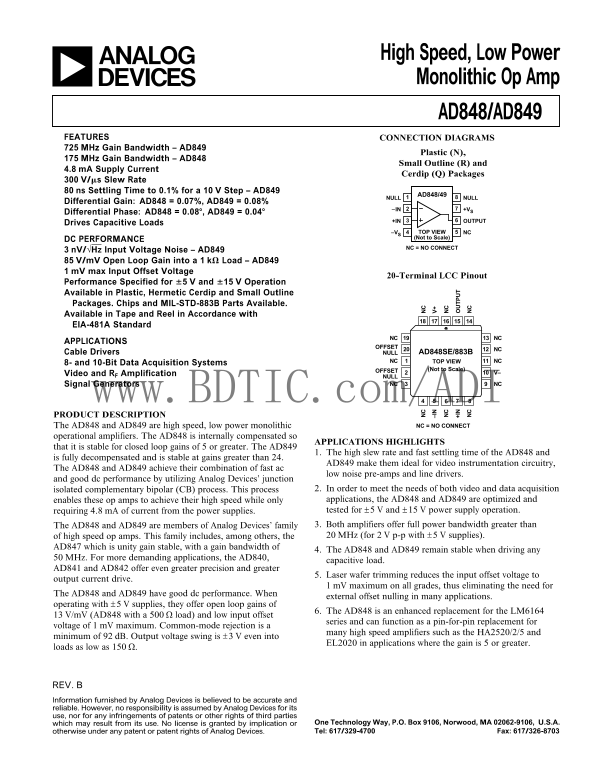
These high-speed, low-power AD848/AD849 operational amplifiers are designed for robust signal amplification in critical analog circuits. Ideal for video instrumentation and data acquisition systems, they offer fast slew rates and excellent stability across varying gain structures. The accompanying manual provides comprehensive technical specifications, detailed connection diagrams, performance curves, and specific application guidance for engineers designing demanding line drivers, preamplifiers, and monitoring equipment.
Page 1 Text Content
High Speed, Low Power Monolithic Op Amp AD848/AD849
FEATURES CONNECTION DIAGRAMS MHz Gain Bandwidth – AD849
Plastic (N),
MHz Gain Bandwidth – AD848
Small Outline (R) and
4.8 m A Supply Current
Cerdip (Q) Packages
V/ms Slew Rate ns Settling Time to 0.1% for a 10 V Step – AD849
AD848/49
NULL NULL
Differential Gain: AD848 = 0.07%, AD849 = 0.08%
–IN +VS
Differential Phase: AD848 = 0.088, AD849 = 0.048
+IN OUTPUT
Drives Capacitive Loads
–VS 5TOP VIEW NC
(Not to Scale)
DC PERFORMANCE
NC = NO CONNECT
n V/√Hz Input Voltage Noise – AD849 V/m V Open Loop Gain into a 1 k V Load – AD849 m V max Input Offset Voltage
20-Terminal LCC Pinout
Performance Specified for 65 V and 615 V Operation Available in Plastic, Hermetic Cerdip and Small Outline Packages. Chips and MIL-STD-883B Parts Available. Available in Tape and Reel in Accordance with EIA-481A Standard
NC NC
APPLICATIONS
OFFSET
Cable Drivers NULL AD848SE/883B
NC TOP VIEW NC
8- and 10-Bit Data Acquisition Systems
OFFSET (Not to Scale)
Video and RF Amplification V–
Signal Generators NC NC
www.BDTIC.com/ADI PRODUCT DESCRIPTION
The AD848 and AD849 are high speed, low power monolithic NC = NO CONNECT
operational amplifiers. The AD848 is internally compensated so
APPLICATIONS HIGHLIGHTS
that it is stable for closed loop gains of 5 or greater. The AD849
1. The high slew rate and fast settling time of the AD848 and
is fully decompensated and is stable at gains greater than 24. +I
AD849 make them ideal for video instrumentation circuitry,
The AD848 and AD849 achieve their combination of fast ac
low noise pre-amps and line drivers.
and good dc performance by utilizing Analog Devices’ junction
isolated complementary bipolar (CB) process. This process 2. In order to meet the needs of both video and data acquisition enables these op amps to achieve their high speed while only applications, the AD848 and AD849 are optimized and requiring 4.8 m A of current from the power supplies. tested for ±5 V and ±15 V power supply operation. The AD848 and AD849 are members of Analog Devices’ family 3. Both amplifiers offer full power bandwidth greater than of high speed op amps. This family includes, among others, the MHz (for 2 V p-p with ±5 V supplies).
AD847 which is unity gain stable, with a gain bandwidth of
4. The AD848 and AD849 remain stable when driving any
MHz. For more demanding applications, the AD840,
capacitive load.
AD841 and AD842 offer even greater precision and greater
5. Laser wafer trimming reduces the input offset voltage to
output current drive.
m V maximum on all grades, thus eliminating the need for
The AD848 and AD849 have good dc performance. When
external offset nulling in many applications.
operating with ±5 V supplies, they offer open loop gains of
6. The AD848 is an enhanced replacement for the LM6164
V/m V (AD848 with a 500 Ω load) and low input offset
series and can function as a pin-for-pin replacement for
voltage of 1 m V maximum. Common-mode rejection is a
many high speed amplifiers such as the HA2520/2/5 and
minimum of 92 d B. Output voltage swing is ±3 V even into
EL2020 in applications where the gain is 5 or greater.
loads as low as 150 Ω.
REV. Information furnished by Analog Devices is believed to be accurate and reliable. However, no responsibility is assumed by Analog Devices for its use, nor for any infringements of patents or other rights of third parties
which may result from its use. No license is granted by implication or One Technology Way, P.O. Box 9106, Norwood, MA 02062-9106, U.S.A. otherwise under any patent or patent rights of Analog Devices. Tel: 617/329-4700 Fax: 617/326-8703
Page Summary Contents For AD848 AD849 Analog Devices Technical Data Sheet and User's Guide
Manual Details
| Brand | Analog Devices |
|---|---|
| Pages | 8 |
| File Size | 237.12 KB |
| Published | June 16, 2026 |
Enter the captcha to get the download link:

Frequently Asked Questions
What are the power supply requirements for optimal operation?
The AD848 and AD849 were tested for both ±5 V and ±15 V power supply operations.
How does the AD848 compare to older models like the LM6164?
The AD848 is an enhanced replacement for the LM6164, offering a low input offset voltage of 1 mV maximum.
Is external compensation needed when using these amplifiers?
No, both AD848 and AD849 are internally compensated; the AD849 is fully decompensated, making it stable at gains greater than 24.
What types of loads can the AD848 drive for video applications?
The AD848 functions well as a high-speed line driver for both terminated and unterminated cables.