# A B C D E F G H I J K L M N O P Q R S T U V W X Y Z

AD8260 Analog Devices Technical Specifications and User Guide

Summary

This high dynamic range analog front-end IC is engineered for advanced signal processing in communications and RF systems, featuring a low-noise preamplifier and digitally programmable VGA. Ideal for transceivers and AGC implementations requiring reliable performance across single/dual supplies and varying gains. The guide provides comprehensive technical details on block diagrams, gain control methods, optimum biasing, and best practices, making it essential reading for engineers designing high-speed, robust signal acquisition systems.
📄 Preview 📖 Table of Contents Contents PAGE OF 32

Page 1 Text Content

High Current Driver Amplifier and Digital VGA/Preamplifier with 3 d B Steps

AD8260 FEATURES FUNCTIONAL BLOCK DIAGRAM

VOCM INPP INRP INRN INPN TXFB VNEG VNEG

High current driver Differential input—direct drive from DAC

Preset gain: 1.5× −3 d B bandwidth: 195 MHz

VMDO TXOP

Large output drive: >±300 m A

GM ×1

VGA/preamplifier TXEN TXOP

HIGH CURRENT DRIVER

Low noise

VMDI AD8260 VPOS

Voltage noise: 2.4 n V/√Hz

Current noise: 5 p A/√Hz

VNCM VPOS

−3 d B bandwidth: 230 MHz BIAS

Gain range: 30 d B in 3 d B steps VPSB VPSR

−6 d B to +24 d B (for preamplifier gain of 6 d B)

VGA/PREAMPLIFIER

Single-ended preamplifier input and differential VGA ENBL

ATTENUATOR

output

VGAP PRAI

Supplies: 3.3 V to 10 V (with VMID enabled) GM STAGES ±3.3 V to ±5 V (with VMID disabled) VGAN

LOGIC

Power: 93 m W with 3.3 V supplies Power-down for VGA, driver amplifier, and system

VNGR VPSR GNS3 GNS2 GNS1 GNS0 PRAO VNGR

APPLICATIONS

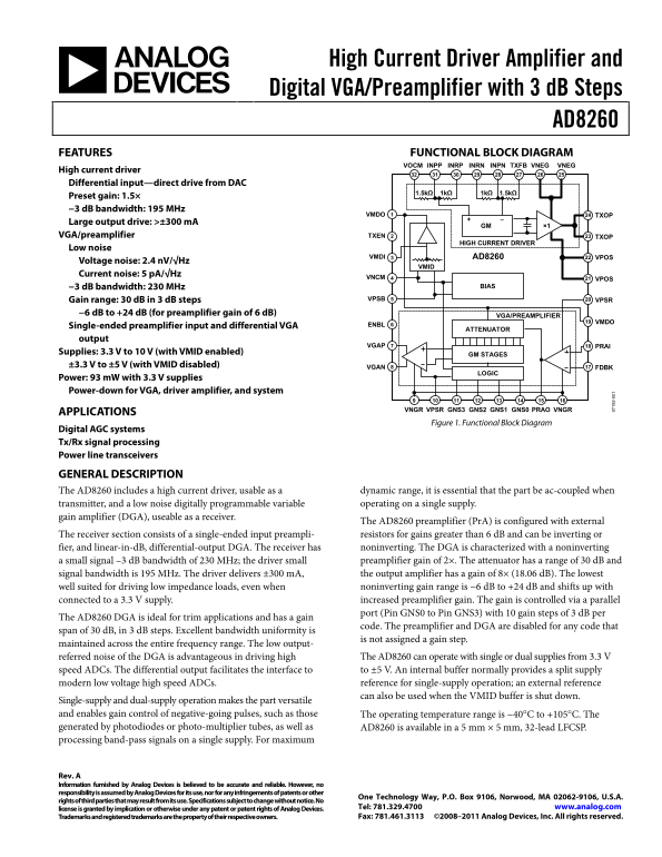
Figure 1. Functional Block Diagram

Digital AGC systems Tx/Rx signal processing Power line transceivers

GENERAL DESCRIPTION

The AD8260 includes a high current driver, usable as a dynamic range, it is essential that the part be ac-coupled when transmitter, and a low noise digitally programmable variable operating on a single supply.

gain amplifier (DGA), useable as a receiver.

The AD8260 preamplifier (Pr A) is configured with external The receiver section consists of a single-ended input preampli- resistors for gains greater than 6 d B and can be inverting or fier, and linear-in-d B, differential-output DGA. The receiver has noninverting. The DGA is characterized with a noninverting a small signal –3 d B bandwidth of 230 MHz; the driver small preamplifier gain of 2×. The attenuator has a range of 30 d B and signal bandwidth is 195 MHz. The driver delivers ±300 m A, the output amplifier has a gain of 8× (18.06 d B). The lowest well suited for driving low impedance loads, even when noninverting gain range is −6 d B to +24 d B and shifts up with connected to a 3.3 V supply. increased preamplifier gain. The gain is controlled via a parallel

port (Pin GNS0 to Pin GNS3) with 10 gain steps of 3 d B per 2-

The AD8260 DGA is ideal for trim applications and has a gain

code. The preamplifier and DGA are disabled for any code that

span of 30 d B, in 3 d B steps. Excellent bandwidth uniformity is

is not assigned a gain step.

maintained across the entire frequency range. The low output-

referred noise of the DGA is advantageous in driving high The AD8260 can operate with single or dual supplies from 3.3 V speed ADCs. The differential output facilitates the interface to to ±5 V. An internal buffer normally provides a split supply modern low voltage high speed ADCs. reference for single-supply operation; an external reference can also be used when the VMID buffer is shut down.

Single-supply and dual-supply operation makes the part versatile and enables gain control of negative-going pulses, such as those The operating temperature range is −40°C to +105°C. The generated by photodiodes or photo-multiplier tubes, as well as AD8260 is available in a 5 mm × 5 mm, 32-lead LFCSP. processing band-pass signals on a single supply. For maximum

Rev. A Information furnished by Analog Devices is believed to be accurate and reliable. However, no responsibility is assumed by Analog Devices for its use, nor for any infringements of patents or other

One Technology Way, P.O. Box 9106, Norwood, MA 02062-9106, U.S.A.

rights of third parties that may result from its use. Specifications subject to change without notice. No

license is granted by implication or otherwise under any patent or patent rights of Analog Devices. Tel: 781.329.4700 www.analog.com Trademarks and registered trademarks are the property of their respective owners. Fax: 781.461.3113 ©2008–2011 Analog Devices, Inc. All rights reserved.

Page Summary Contents For AD8260 Analog Devices Technical Specifications and User Guide

Page 1 High Current Driver Amplifier and Digital VGA/Preamplifier with 3 d B Steps AD8260 FEATURES FUNCTIONAL BLOCK DIAGRAM VOCM INPP INRP INRN INPN TXFB VNEG VNEG High current driver Differential input—dire...
Page 2 AD8260 TABLE OF CONTENTS Features .............................................................................................. 1 VMID Buffer ............................................................
Page 3 AD8260 SPECIFICATIONS VS (supply voltage) = 3.3 V, TA = 25°C, preamplifier gain = 2× (RFB1 = RFB2 = 100 Ω), VVMDO = VS/2, f = 10 MHz, CL = 5 p F, RLOAD = 500 Ω, DGA differential output. All d Bm value...
Page 4 AD8260 Parameter Conditions Min Typ Max Unit Output Third-Order Intercept, RLOAD = 50 Ω VOUT = 1 V p-p, f = 10 MHz 33 d Bm VOUT = 2 V p-p, f = 10 MHz 40 d Bm VOUT = 1 V p-p, f = 45 MHz 23 d Bm VOUT = ...
Page 5 AD8260 Parameter Conditions Min Typ Max Unit ACCURACY Absolute Gain Error All gain codes, limits are 3σ −0.5 ±0.15 +0.5 d B Gain Law Conformance (DNL) Differential gain error code-to-code −0.3 ±0.15 +...
Page 6 AD8260 ABSOLUTE MAXIMUM RATINGS Table 2. Parameter Rating Stresses above those listed under Absolute Maximum Ratings Voltage may cause permanent damage to the device. This is a stress Supply Voltage (...
Page 7 AD8260 PIN CONFIGURATION AND FUNCTION DESCRIPTIONS VMDO TXOP PIN 1 TXEN INDICATOR TXOP VMDI VPOS VNCM AD8260 VPOS VPSB TOP VIEW VPSR (Not to Scale) ENBL VMDO VGAP PRAI VGAN FDBK NOTES 1. THE EXPOSED P...
Page 8 AD8260 IN (d IN (d IN (d TYPICAL PERFORMANCE CHARACTERISTICS VS (supply voltage) = 3.3 V, TA = 25°C, CL = 5 p F, f = 10 MHz, preamplifier gain = 2×, RFB1 and RFB2 of the preamplifier = 100 Ω, RLOAD of...
Page 9 AD8260 IC IS TO TI (d c) IC IS TO TI (d c) IC IS TO TI (d c) f = 10MHz –30 HD2, VOUT = 1V p-p HD3, VOUT = 1V p-p HD2, VOUT = 2V p-p RLOAD = 50Ω, VOUT = 1V p-p HD3, VOUT = 2V p-p RLOAD = 50Ω, VOUT = 2V...
Page 10 TP VO LT (V TP VO LT (V TP (d AD8260 CLOAD = 5p F 0.15 CLOAD = 10p F CLOAD = 47p F –0.15 RLOAD = 50Ω –80 NONINVERTING TIME (ns) FREQUENCY (MHz) Figure 15. Missing Tone Power Ratio for the High Current...
Page 11 AD8260 IN TE (d TP VO LT (V IN (d 2.0 1.00 RLOAD 50Ω NONINVERTING CLOAD 5p F 1.5 CLOAD = 10p F 0.75 CLOAD = 47p F AVERAGE OF 3 SAMPLES 1.0 0.50 f = 1MHz, 10MHz, AND 40MHz 10–30 30–10 807060–20 TIME (n...
Page 12 IF FE EN TI IN (d IF FE EN TI IN (d IF FE EN TI IN (d AD8260 FREQUENCY (Hz) FREQUENCY (Hz) Figure 27. Frequency Response for a Supply Voltage (VS) of 3.3 V for all Codes 2- Figure 30. Group Delay vs. ...
Page 13 AD8260 SH T- IR IT IN PU T- EF ER ED IS TP T- EF ER ED IS (n V/ √H z) (n V/ √H z) IN PU T- EF ER ED IS (n V/ √H z) VOUT = 1V p-p GAIN CODE = 1011 GAIN CODE = 0110 HD2 HD3 FREQUENCY (Hz) LOAD RESISTANC...
Page 14 IP (d IM (d c) IC IS TO TI (d c) AD8260 GAIN CODE = 1011 IP1d B LIMITED AT LOW GAIN BY THE VOUT = 1V p-p DYNAMIC RANGE OF THE PREAMPLIFIER HD2 –5 HD3 –100 1MHz 10MHz FREQUENCY (Hz) GAIN SELECT CODE Fi...
Page 15 AD8260 TP VO LT (V TP VO LT (V +SUPPLY VGA/PREAMPLIFIER 1.0 –20 +SUPPLY HIGH CURRENT DRIVER –SUPPLY VGA PREAMPLIFIER VS = +3V, +5V, AND ±5V –SUPPLY HIGH CURRENT DRIVER VS = ±3.3V GAIN CODE = 1011 TIME...
Page 16 AD8260 TEST CIRCUITS NETWORK ANALYZER 50Ω 50Ω INOUT AD8260—HIGH CURRENT DRIVER 0.1µF INRN TXFB TXOP 453Ω Figure 51. Test Circuit for Frequency Response of the High Current Driver AD8260—HIGH CURRENT D...
Page 17 AD8260 SIGNAL GENERATORS AD8260—HIGH CURRENT DRIVER SPECTRUM 50Ω ANALYZER 1:1 INRN TXFB TXOP 453Ω IN 50Ω INRP Figure 55. Test Circuit for IMD3 and OIP3 of the High Current Driver AD8260—HIGH CURRENT D...
Page 18 AD8260 NETWORK ANALYZER AD8260—VGA/PREAMPLIFIER PREAMP Figure 59. Test Circuit for Frequency Response and Group Delay of the VGA/Preamplifier NETWORK ANALYZER WITH S-PARAMETER CAPABILITY AD8260—VGA/ P...
Page 19 AD8260 SPECTRUM ANALYZER AD8260—VGA/PREAMPLIFIER LP FILTER 0.1µF 50Ω50Ω PREAMP SIGNAL GENERATOR Figure 62. Test Circuit for Harmonic Distortion Measurements of the VGA/Preamplifier AD8260—VGA/PREAMPLI...
Page 20 AD8260 THEORY OF OPERATION 4-bit parallel interface. Figure 64 shows the circuit block OVERVIEW diagram and basic application connections, and illustrates the The AD8260 is a self-contained transceive...
Page 21 AD8260 1V MAX WITH 1.8V OR 3.3V 200m A pk 20m A DAC OPTIONAL USER SELECTED CFB REDUCES HF PEAKING 0.1µF0.1µF50Ω WITH CAPACITIVE LOADING VOCM INPP 1.5kΩ 1kΩ 1kΩ 1.5kΩ OPTIONAL CLAMP DIODES VMDO TXOP AN...
Page 22 AD8260 PRECAUTIONS TO BE OBSERVED DURING HALF- determine the −3 d B bandwidth of the amplifier. Smaller DUPLEX OPERATION resistor values may compromise preamplifier stability. During receive, when the...
Page 23 AD8260 Assuming RS = 0, RFB1 = RFB2 = 100 Ω, At = 16, and AVGA = 8, the Table 4. Gain Control Logic Table noise simplifies to D3 D2 D1 D0 Function Comments 0 0 0 0 Disable Pr A and DGA powered down )8...
Page 24 AD8260 SINGLE-SUPPLY OPERATION AND AC COUPLING active first to listen to any signals, and the driver needs to be off. Therefore, the gain code should be set to 0001 (−6 d B When operating the AD8260 f...
Page 25 AD8260 APPLICATIONS INFORMATION CONTROLLER The AD8260 is ideally suited for compact applications requiring MICROPROCESSOR + high frequency and large current drive of complex modulation MODULATOR produ...
Page 26 AD8260 EVALUATION BOARD Analog Devices provides evaluation boards to customers as a PCB artwork for all conductor and silkscreen layers is shown in support service so that the circuit designer can bec...
Page 27 AD8260 DEFAULT GAIN SETTING CONNECTING THE EVALUATION BOARD COMPONENTS ARE SHOWN IN BLACK, OPTIONAL COMPONENTS Figure 69 shows an evaluation board with typical test connec- ARE SHOWN IN GRAY. tions. T...
Page 28 AD8260 PULSE GENERATOR WITH DIFFERENTIAL OUTPUT HIGH CURRENT DRIVER INPUTS VGA OUTPUT HIGH (TO SCOPE) CURRENT DRIVER RLOAD OUTPUT SINGLE- ENDED VGA INPUT POWER SUPPLY FUNCTION GENERATOR FOR VGA INPUT ...
Page 29 AD8260 GND –VS+VS INRP INRN –VS+VS GND1 GND4GND3GND2 GND6GND5 DNI FB R17 R15 C1 C2 DNI DNI R14 DNI 0.1µF TXOPR9 R16 DNI VP SR R21 IN PP TXOP_1 IN S2 IN TXENVPSB S1 IN PN VMDO TXOP L6 EN 120n H S0 TX F...
Page 30 AD8260 Figure 71. AD8260-EVALZ Component Side Assembly Figure 73. AD8260-EVALZ Secondary Side Copper Figure 72. AD8260-EVALZ Component Side Copper Figure 74. AD8260-EVALZ Power Plane Rev. A | Page 30 ...
Page 31 AD8260 Figure 75. AD8260-EVALZ Ground Plane Figure 76. Component Side Silkscreen Rev. A | Page 31 of 32
Page 32 AD8260 OUTLINE DIMENSIONS 0.60 MAX BSC SQ 0.60 MAX PIN INDICATOR PIN 0.50 INDICATOR BSC EXPOSED 2.85 BSC SQ PAD 2.70 SQ (BOTTOM VIEW) 2.55 0.20 MIN 3.50 REF 0.80 MAX 1.00 12° MAX 0.65 TYP 0.85 FOR PRO...

Manual Details

Brand Analog Devices
Pages 32
File Size 1.54 MB
Published May 14, 2026
200 views

Enter the captcha to get the download link:

captcha

Frequently Asked Questions

What operational temperature range does the AD8260 support?

The operating temperature range is −40°C to +105°C.

Can the AD8260 operate using single or dual supplies?

Yes, it can operate with single or dual supplies from 3.3 V up to ±5 V.

What are the bandwidth specifications for the preamplifier and driver?

The small signal –3 dB bandwidth is 230 MHz for the DGA, and the attenuator has a signal bandwidth of 195 MHz.

How is negative-going pulse gain controlled on this device?

Gain control can enable the gain of negative-going pulses (e.g., those from photodiodes) in addition to positive ones.