# A B C D E F G H I J K L M N O P Q R S T U V W X Y Z

ADP5037 Analog Devices Technical Data Sheet / Manual

Summary

The ADP5037 is a compact, high-performance power management unit featuring two 800mA buck regulators and two 300mA LDOs in a small 4mm x 4mm package. This solution delivers stable, energy-efficient power for complex portable electronics, including medical devices and industrial instrumentation. The accompanying manual provides comprehensive technical details necessary for design engineers, covering operating modes (PWM/PSM), component selection, and detailed specifications to ensure optimal performance in space-constrained applications.
📄 Preview 📖 Table of Contents Contents PAGE OF 28

Page 1 Text Content

Dual 3 MHz, 800 m A Buck Regulators with Two 300 m A LDOs

Data Sheet ADP5037

FEATURES 4 mm LFCSP to meet demanding performance and board space requirements.

Main input voltage range: 2.3 V to 5.5 V

Two 800 m A buck regulators and two 300 m A LDOs The high switching frequency of the buck regulators enables tiny 24-lead, 4 mm × 4 mm LFCSP package multilayer external components and minimizes the board space. Regulator accuracy: ±3% When the MODE pin is set high, the buck regulators operate in

Factory programmable or external adjustable VOUTx forced PWM mode. When the MODE pin is set low and the 3 MHz buck operation with forced PWM and auto PWM/PSM load is above a predefined threshold, the buck regulators modes operate in PWM mode. When the load current falls below a BUCK1/BUCK2: output voltage range from 0.8 V to 3.8 V predefined threshold, the regulator operates in power save LDO1/LDO2: output voltage range from 0.8 V to 4.75 V mode (PSM), improving the light-load efficiency. LDO1/LDO2: low input supply voltage from 1.7 V to 5.5 V

The two bucks operate out of phase to reduce the input capaci-

LDO1/LDO2: high PSRR and low output noise

tor requirement. The low quiescent current, low dropout voltage, APPLICATIONS and wide input voltage range of the ADP5037 LDOs extend the battery life of portable devices. The ADP5037 LDOs maintain

Power for processors, ASICS, FPGAs, and RF chipsets

power supply rejection greater than 60 d B for frequencies as

Portable instrumentation and medical devices

high as 10 k Hz while operating with a low headroom voltage.

Space constrained devices

Regulators in the ADP5037 are activated though dedicated

GENERAL DESCRIPTION

enable pins. The default output voltages can be externally set in

The ADP5037 combines two high performance buck regulators

the adjustable version or factory programmable to a wide range

and two low dropout (LDO) regulators in a small, 24-lead 4 mm ×

of preset values in the fixed voltage version.

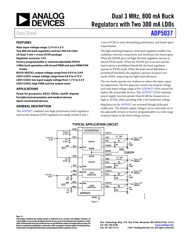
TYPICAL APPLICATION CIRCUIT AVIN

HOUSEKEEPING

CAVIN

VOUT1

VIN1 SW1

2.3V TO VOUT1 AT

FB1 R1

4.7µF BUCK1

PGND1 10µF

ON EN1

OFF EN1 MODE

PSM/PWM

VOUT2

VIN2 MODE

C2 SW2 VOUT2 AT

BUCK2 FB2 R3

EN2 R4

EN2 PGND2 10µF

EN3 VOUT3 VOUT3 AT

EN3 LDO1 300m A

VIN3 FB3 R5

1.7V TO (ANALOG)

1µF ON EN4

VOUT4 VOUT4 AT

LDO2 300m A

FB4 R7

(DIGITAL) C8

ADP5037

Figure 1.

Rev. 0 Information furnished by Analog Devices is believed to be accurate and reliable. However, no responsibility is assumed by Analog Devices for its use, nor for any infringements of patents or other

One Technology Way, P.O. Box 9106, Norwood, MA 02062-9106, U.S.A.

rights of third parties that may result from its use. Specifications subject to change without notice. No

license is granted by implication or otherwise under any patent or patent rights of Analog Devices. Tel: 781.329.4700 www.analog.com Trademarks and registered trademarks are the property of their respective owners. Fax: 781.461.3113 ©2011 Analog Devices, Inc. All rights reserved.

Page Summary Contents For ADP5037 Analog Devices Technical Data Sheet / Manual

Page 1 Dual 3 MHz, 800 m A Buck Regulators with Two 300 m A LDOs Data Sheet ADP5037 FEATURES 4 mm LFCSP to meet demanding performance and board space requirements. Main input voltage range: 2.3 V to 5.5 V Tw...
Page 2 ADP5037 Data Sheet TABLE OF CONTENTS Features .............................................................................................. 1  Power Dissipation and Thermal Considerations ..............
Page 3 Data Sheet ADP5037 SPECIFICATIONS GENERAL SPECIFICATIONS VAVIN = VIN1 = VIN2 = 2.3 V to 5.5 V; VIN3 = VIN4 = 1.7 V to 5.5 V; TJ = −40°C to +125°C for minimum/maximum specifications, and TA = 25°C for ...
Page 4 ADP5037 Data Sheet BUCK1 AND BUCK2 SPECIFICATIONS VAVIN = VIN1 = VIN2 = 2.3 V to 5.5 V; TJ = −40°C to +125°C for minimum/maximum specifications, and TA = 25°C for typical specifications, unless otherw...
Page 5 Data Sheet ADP5037 Parameter Symbol Test Conditions/Comments Min Typ Max Unit VOLTAGE FEEDBACK VFB3, VFB4 0.485 0.5 0.515 V DROPOUT VOLTAGE4 VDROPOUT VOUT3 = VOUT4 = 3.3 V, IOUT3 = IOUT4 = 300 m A 75 ...
Page 6 ADP5037 Data Sheet ABSOLUTE MAXIMUM RATINGS THERMAL RESISTANCE Table 5. Parameter Rating θJA is specified for the worst-case conditions, that is, a device AVIN to AGND −0.3 V to +6 V soldered in a cir...
Page 7 Data Sheet ADP5037 PIN CONFIGURATION AND FUNCTION DESCRIPTIONS PIN 1 FB4 INDICATOR AGND EN4 AVIN VIN2 ADP5037 VIN1 SW2 TOP VIEW SW1 (Not to Scale) PGND2 PGND1 NC MODE NOTES 1. NC = NO CONNECT. DO NOT ...
Page 8 ADP5037 Data Sheet TYPICAL PERFORMANCE CHARACTERISTICS VIN1= VIN2 = VIN3= VIN4 = 3.6 V, TA = 25°C, unless otherwise noted. VIN = 3.6V, +25°C VIN = 3.6V, +85°C VIN = 3.6V, –40°C INPUT VOLTAGE (V) IOUT ...
Page 9 Data Sheet ADP5037 IC IE IC IE IC IE VIN = 3.9V VIN = 3.6V VIN = 4.2V VIN = 2.3V VIN = 5.5V VIN = 5.5V VIN = 4.2V IOUT (A) IOUT (A) Figure 9. BUCK1 Efficiency vs. Load Current, Across Input Voltage, F...
Page 10 IC IE IC IE IC IE ADP5037 Data Sheet IOUT (A) IOUT (A) Figure 15. BUCK1 Efficiency vs. Load Current, Across Temperature, Figure 18. BUCK2 Switching Frequency vs. Output Current, Across VIN = 3.9 V, VO...
Page 11 Data Sheet ADP5037 SW SW CH1 50m V CH2 500m A Ω M 400ns A CH2 220m A CH1 50.0m V M 1.00ms A CH3 4.80V CH4 2.00V CH3 1.00V CH4 2.00V Figure 21. Typical Waveforms, VOUT1 = 3.3 V, IOUT1 = 30 m A, PWM Mod...
Page 12 ADP5037 Data Sheet CH1 50.0m V CH2 200m A Ω M 20.0µs A CH2 408m A CH1 2.00V CH2 50.0m A 40.0µs CH3 2.2V CH4 5.00V CH3 5.00V Figure 27. BUCK1 Response to Load Transient, IOUT1 from 20 m A to 180 m A, 7...
Page 13 Data Sheet ADP5037 INPUT VOLTAGE (V) LOAD CURRENT (A) Figure 33. PMOS RDSON vs. Input Voltage Across Temperature Figure 36. LDO Ground Current vs. Output Load, VIN3 = 3.3 V, VOUT3 = 2.8 V VIN = 4.2V, ...
Page 14 ADP5037 Data Sheet IS IS VIN = 5V VIN = 3.3V 0.001 0.01 0.1 1k 10k 100k 1M 10M ILOAD (m A) FREQUENCY (Hz) Figure 39. LDO Output Noise vs. Load Current, Across Input Voltage, Figure 42. LDO PSRR Across...
Page 15 Data Sheet ADP5037 POWER DISSIPATION AND THERMAL CONSIDERATIONS The ADP5037 is a highly efficient μPMU, and, in most cases, BUCK REGULATOR POWER DISSIPATION the power dissipated in the device is not a...
Page 16 ADP5037 Data Sheet Switching losses are associated with the current drawn by the JUNCTION TEMPERATURE driver to turn on and turn off the power devices at the switching In cases where the board tempera...
Page 17 Data Sheet ADP5037 THEORY OF OPERATION VOUT1 FB1 FB2 VOUT2 GM ERROR GM ERROR ENBK2 AVIN 75ΩENBK1 75Ω AMP AMP PWM PWM COMP COMP VIN1 SOFT START SOFT START VIN2 ILIMIT ILIMIT PSM PSM COMP COMP PWM/ PWM/...
Page 18 ADP5037 Data Sheet Thermal Protection Alternatively, the user can select device models with a UVLO set at a higher level, suitable for USB applications. For these In the event that the junction temper...
Page 19 Data Sheet ADP5037 BUCK1 AND BUCK2 drives the inductor to make the output voltage rise again to the upper threshold. This process is repeated while the load current The buck uses a fixed frequency and...
Page 20 ADP5037 Data Sheet the input conditions change again and the required duty cycle Each LDO output voltage is set through external resistor falls, the buck immediately restarts PWM regulation without di...
Page 21 Data Sheet ADP5037 APPLICATIONS INFORMATION BUCK EXTERNAL COMPONENT SELECTION Ceramic capacitors are manufactured with a variety of dielec- trics, each with a different behavior over temperature and T...
Page 22 ADP5037 Data Sheet The peak-to-peak output voltage ripple for the selected output To minimize supply noise, place the input capacitor as close as capacitor and inductor values is calculated using the ...
Page 23 Data Sheet ADP5037 LDO EXTERNAL COMPONENT SELECTION temperature range and is not a function of package or voltage rating. Feedback Resistors For the adjustable model, the maximum value of Rb is not to...
Page 24 ADP5037 Data Sheet PCB LAYOUT GUIDELINES Poor layout can affect ADP5037 performance, causing electro-  Maximize the size of ground metal on the component side magnetic interference (EMI) and electrom...
Page 25 Data Sheet ADP5037 TYPICAL APPLICATION SCHEMATICS HOUSEKEEPING CAVIN VOUT1 2.3V TO VIN1 SW1 VOUT1 @ FB1 800m A 4.7µF BUCK1 ON PGND1 10µF EN1 OFF EN1 MODE PWM PSM/PWM VOUT2 VIN2 MODE C2 SW2 VOUT2 @ 4.7...
Page 26 ADP5037 Data Sheet BILL OF MATERIALS Table 12. Reference Value Part Number Vendor Package or Dimension (mm) CAVIN 0.1 μF, X5R, 6.3 V JMK105BJ104MV-F Taiyo-Yuden 0402 C3, C4, C7, C8 1 μF, X5R, 6.3 V LM...
Page 27 Data Sheet ADP5037 OUTLINE DIMENSIONS 4.10 0.30 4.00 SQ 0.25 PIN 3.90 0.20 INDICATOR INDICATOR 0.50 BSC EXPOSED 2.20 PAD 2.10 SQ 2.00 0.50 0.25 MIN VIEW 0.40 VIEWTOP FOR PROPER CONNECTION OF THE EXPOS...
Page 28 ADP5037 Data Sheet NOTES ©2011 Analog Devices, Inc. All rights reserved. Trademarks and registered trademarks are the property of their respective owners. D09887-0-8/11(0) Rev. 0 | Page 28 of 28

Manual Details

Brand Analog Devices
Pages 28
File Size 619.00 KB
Published June 15, 2026
6 views

Enter the captcha to get the download link:

captcha

Frequently Asked Questions

What is the operating voltage range for this regulator?

The main input voltage range is from 2.3 V to 5.5 V.

How do I ensure low power consumption during light loads?

When the load current drops below a predefined threshold, the buck regulators enter Power Save Mode (PSM), improving efficiency.

What type of package does the ADP5037 use?

It uses a 24-lead, 4 mm × 4 mm LFCSP package for minimal board space.

Is this chip suitable for battery-powered medical devices?

Yes, its low quiescent current and wide input range extend battery life in portable and medical instruments.