AD7112 LC 2 MOS LOGDAC Dual Logarithmic DA Converter Data Sheet Manual User Guide
Summary
The AD7112 is a high-performance dual logarithmic D/A converter designed for advanced signal processing applications, featuring an exceptional 88.5 dB dynamic range and fine 0.375 dB resolution. This manual serves as essential technical documentation, detailing pin compatibility (with the industry standard AD7528), electrical specifications, functional block diagrams, and detailed application guidelines. It is ideal for electronics engineers developing systems for sonar, audio attenuation, or specialized function generators requiring high precision and excellent DAC matching.
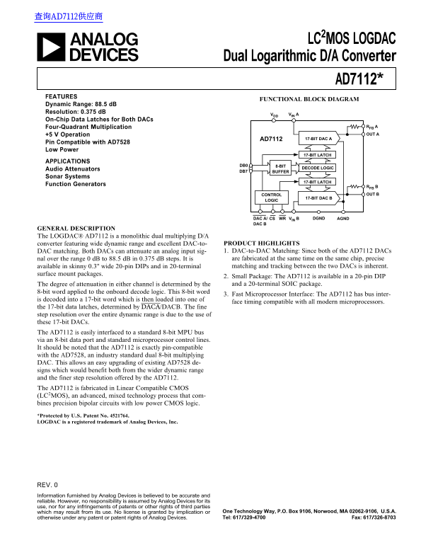
Page 1 Text Content
查询AD7112供应商
LC2MOS LOGDAC
Dual Logarithmic D/A Converter
AD7112*
FEATURES
FUNCTIONAL BLOCK DIAGRAM
Dynamic Range: 88.5 d B Resolution: 0.375 d B
VDD VIN A
On-Chip Data Latches for Both DACs
Four-Quadrant Multiplication RFB A +5 V Operation OUT A
17-BIT DAC AAD7112
Pin Compatible with AD7528 Low Power
17-BIT LATCH
APPLICATIONS
DB0 8-BIT
DECODE LOGIC
Audio Attenuators
DB7 BUFFER
Sonar Systems
17-BIT LATCH
Function Generators
RFB B
CONTROL OUT B
17-BIT DAC B
LOGIC
DAC A/ WR VIN B AGNDDGNDCS DAC B
GENERAL DESCRIPTION The LOGDAC® AD7112 is a monolithic dual multiplying D/A
converter featuring wide dynamic range and excellent DAC-to- PRODUCT HIGHLIGHTS DAC matching. Both DACs can attenuate an analog input sig- 1. DAC-to-DAC Matching: Since both of the AD7112 DACs nal over the range 0 d B to 88.5 d B in 0.375 d B steps. It is are fabricated at the same time on the same chip, precise available in skinny 0.3" wide 20-pin DIPs and in 20-terminal matching and tracking between the two DACs is inherent.
surface mount packages.
2. Small Package: The AD7112 is available in a 20-pin DIP The degree of attenuation in either channel is determined by the and a 20-terminal SOIC package.
8-bit word applied to the onboard decode logic. This 8-bit word
3. Fast Microprocessor Interface: The AD7112 has bus inter-
is decoded into a 17-bit word which is then loaded into one of
face timing compatible with all modern microprocessors.
the 17-bit data latches, determined by DACA/DACB. The fine step resolution over the entire dynamic range is due to the use of these 17-bit DACs. The AD7112 is easily interfaced to a standard 8-bit MPU bus via an 8-bit data port and standard microprocessor control lines. It should be noted that the AD7112 is exactly pin-compatible with the AD7528, an industry standard dual 8-bit multiplying DAC. This allows an easy upgrading of existing AD7528 de- signs which would benefit both from the wider dynamic range and the finer step resolution offered by the AD7112. The AD7112 is fabricated in Linear Compatible CMOS (LC2MOS), an advanced, mixed technology process that com- bines precision bipolar circuits with low power CMOS logic.
*Protected by U.S. Patent No. 4521764. LOGDAC is a registered trademark of Analog Devices, Inc.
REV. Information furnished by Analog Devices is believed to be accurate and reliable. However, no responsibility is assumed by Analog Devices for its use, nor for any infringements of patents or other rights of third parties
which may result from its use. No license is granted by implication or One Technology Way, P.O. Box 9106, Norwood, MA 02062-9106, U.S.A. otherwise under any patent or patent rights of Analog Devices. Tel: 617/329-4700 Fax: 617/326-8703
Page Summary Contents For AD7112 LC 2 MOS LOGDAC Dual Logarithmic DA Converter Data Sheet Manual User Guide
Manual Details
| Brand | Dual |
|---|---|
| Pages | 12 |
| File Size | 236.09 KB |
| Published | May 30, 2026 |
Enter the captcha to get the download link:
