User Guide for FAIRCHILD AN-8039 in Automotive Systems
Summary
The FDDS100H06_F085 is an AECQ101-grade, smart high-side switch built for managing medium power electrical loads in modern automotive systems. This application note provides comprehensive technical details on its operation, including advanced single and multi-load circuits, micro-controller compatible logic interfaces (3V–5V), and robust diagnostic capabilities. It thoroughly explains features like open-load detection, over-current protection, and autonomous self-protection. Ideal for engineers developing sophisticated power distribution and electrical control units requiring reliable load management and comprehensive fault monitoring.
Page 1 Text Content
www.fairchildsemi.com
AN-8039 Using the FDDS100H06_F085 in Automotive Systems Background
Pin Functions
Smart high-side switches are a standard building block in
IN - The input pin can be driven with a 3V to 5V logic level
today’s automotive power distribution and electrical control
output from devices like microcontrollers, provided the VOH
systems. High and medium current devices with diagnostic
output at 3V conforms to the VOHmin > 2.9V as specified for
features have virtually eliminated fuses and resettable
typical HC logic families (see example VOH minimum for the
breakers in load management.
74VHC00).
In power distribution, single circuits and the associated
ST - The status output is an open-drain configuration and
wiring are protected using smart high-side switches. In
requires a pull-up resistor. This allows multiple devices to
body, lighting, and power train; individual loads are driven
be wire OR’ed where multiple loads do not require
with smart devices that may include diagnostics using
individual diagnostic recognition. Open-load detection can
current sensing, and/or fixed parameter diagnostics with
still be accomplished individually by polling of the input
status feedback, and/or self-protection features.
and status pins.
Autonomous self-protection is almost universal.
The output minimum voltage specified on the status pin relates to the Zener protection diode and is compatible with
Medium Power Load Management
3V to 5V logic levels. This should be pulled up to the logic
The FDDS100H06_F085 is an AECQ101-grade, smart, VCC voltage. high-side switch designed to drive medium power electrical
VBB – The tab and pin 3 are electrically common; however,
loads and provide diagnostic feedback with a
pin 3 is a cut lead and not used for electrical connection.
microprocessor-compatible logic level interface. This
Therefore, power for the device must be provided at the tab.
includes fixed limits for open-load, over-current, and other
The tab pad can also be used with thermal vias and
failure conditions indicated via a status line. There are also
additional PCB radiation area for heat dissipation.
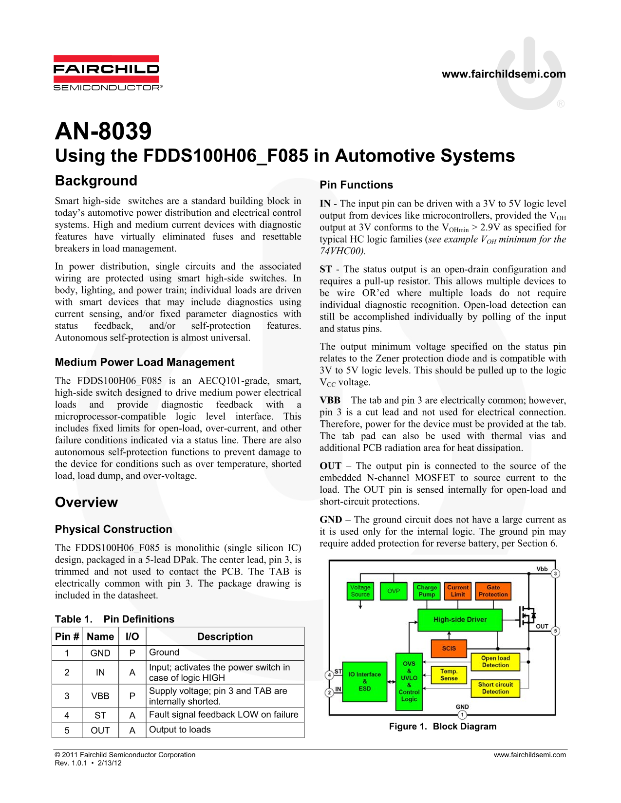
autonomous self-protection functions to prevent damage to the device for conditions such as over temperature, shorted OUT – The output pin is connected to the source of the load, load dump, and over-voltage. embedded N-channel MOSFET to source current to the
load. The OUT pin is sensed internally for open-load and Overview short-circuit protections. GND – The ground circuit does not have a large current as
Physical Construction it is used only for the internal logic. The ground pin may
require added protection for reverse battery, per Section 6.
The FDDS100H06_F085 is monolithic (single silicon IC) design, packaged in a 5-lead DPak. The center lead, pin 3, is trimmed and not used to contact the PCB. The TAB is electrically common with pin 3. The package drawing is included in the datasheet.
Table 1. Pin Definitions Pin # Name I/O Description 1 GND P Ground
Input; activates the power switch in
2 IN A
case of logic HIGH Supply voltage; pin 3 and TAB are
3 VBB P
internally shorted.
4 ST A Fault signal feedback LOW on failure
Figure 1. Block Diagram
5 OUT A Output to loads
© 2011 Fairchild Semiconductor Corporation www.fairchildsemi.com Rev. 1.0.1 • 2/13/12
Page Summary Contents For User Guide for FAIRCHILD AN-8039 in Automotive Systems
Manual Details
| Brand | Fairchild |
|---|---|
| Pages | 13 |
| File Size | 605.34 KB |
| Published | July 15, 2026 |
Enter the captcha to get the download link:

Frequently Asked Questions
What components are needed to stabilize the VBB supply voltage?
You should bypass high-frequency noise using local ceramic capacitors for each device, and a bulk capacitor C1 may be used to stabilize the supply.
How is the status output signal provided by this switch?
The ST output pin is an open-drain configuration that provides fault signals for conditions like open-load, over-current, and over-voltage through its status line.
Do I need external components for the status feedback pin?
Yes, because the status output is an open-drain configuration, it requires a pull-up resistor to function correctly.
What should be done regarding pin 3 during circuit design?
Pin 3 is described as a cut lead and is not used for electrical connection to the PCB; the TAB pad is electrically common with Pin 3.