Texas Instruments TL1453C Data Handbook
Summary
Technical datasheet for Texas Instruments TL1453C dual pulse-width-modulation (PWM) control circuit incorporating complete power control circuitry on single monolithic chip. Designed primarily for power supply control, features on-chip 2.5-V regulator, two error amplifiers, adjustable oscillator (up to 500kHz), two dead-time comparators, undervoltage lockout circuitry, and dual common-emitter output transistor circuits. Uncommitted output transistors provide common-emitter output capability for
Page 1 Text Content
查询TL1453供应商 TL1453C
DUAL PULSE-WIDTH-MODULATION CONTROL CIRCUIT
SLVS039A – FEBRUARY 1990 – REVISED DECEMBER 1990
Complete PWM Power Control Circuitry N OR NS PACKAGE (T0P VIEW)
Completely Synchronized Operation Internal Undervoltage Lockout Protection REF
Wide Supply Voltage Range RT SCP ERROR IN+ IN+ ERROR
Oscillator Frequency 500 k Hz Max
AMPLIFIER 1 IN– IN– AMPLIFIER 2
Variable Dead Time Provides Control
1 FEEDBACK 2 FEEDBACK
Over Total Range
1 DEAD-TIME CONTROL 2 DEAD-TIME CONTROL
Internal Regulator Provides a Stable 2.5-V
1 OUTPUT 2 OUTPUT
Reference Supply
GND VCC
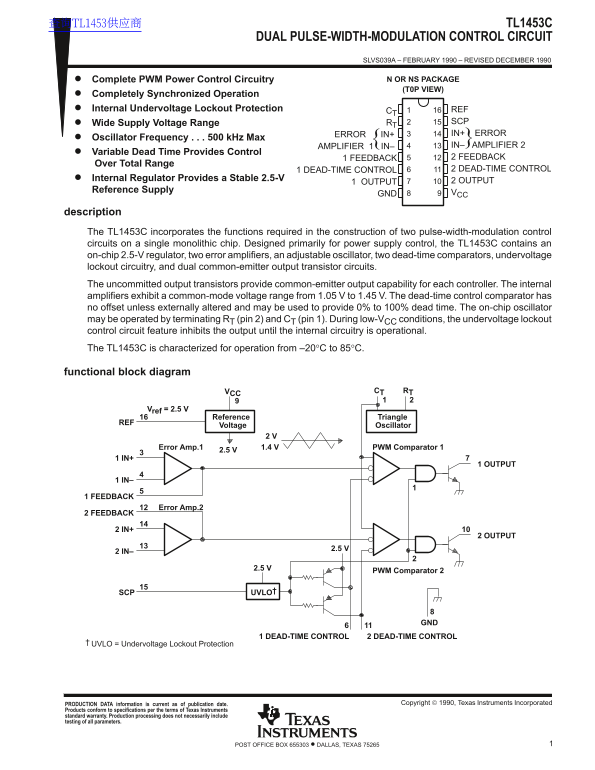
description The TL1453C incorporates the functions required in the construction of two pulse-width-modulation control circuits on a single monolithic chip. Designed primarily for power supply control, the TL1453C contains an on-chip 2.5-V regulator, two error amplifiers, an adjustable oscillator, two dead-time comparators, undervoltage lockout circuitry, and dual common-emitter output transistor circuits. The uncommitted output transistors provide common-emitter output capability for each controller. The internal amplifiers exhibit a common-mode voltage range from 1.05 V to 1.45 V. The dead-time control comparator has no offset unless externally altered and may be used to provide 0% to 100% dead time. The on-chip oscillator may be operated by terminating RT (pin 2) and CT (pin 1). During low-VCC conditions, the undervoltage lockout control circuit feature inhibits the output until the internal circuitry is operational. The TL1453C is characterized for operation from –20°C to 85°C.
functional block diagram
VCC CT RT
Vref = 2.5 V
Reference Triangle
Voltage Oscillator
Error Amp.1 1.4 V PWM Comparator 1
1 IN+
1 OUTPUT
1 IN–
1 FEEDBACK
Error Amp.2
2 FEEDBACK
2 IN+
2 OUTPUT
2 IN–
PWM Comparator 2
SCP UVLO†
1 DEAD-TIME CONTROL 2 DEAD-TIME CONTROL
UVLO = Undervoltage Lockout Protection
Copyright 1990, Texas Instruments Incorporated PRODUCTION DATA information is current as of publication date.
Products conform to specifications per the terms of Texas Instruments standard warranty. Production processing does not necessarily include testing of all parameters.
1POST OFFICE BOX 655303 • DALLAS, TEXAS 75265
Page Summary Contents For Texas Instruments TL1453C Data Handbook
Manual Details
| Brand | Texas Instruments |
|---|---|
| Pages | 7 |
| File Size | 101.36 KB |
| Published | June 19, 2026 |
Enter the captcha to get the download link:

Frequently Asked Questions
What is the recommended supply voltage range for operation?
The recommended supply voltage (VCC) range is 3.6 V to 40 V.
How can I set up or terminate the internal oscillator frequency?
The on-chip oscillator may be operated by terminating R (pin 2) and C (pin 1).
Is there protection against low voltage conditions?
Yes, the Undervoltage Lockout (UVLO) circuit feature inhibits the output until the internal circuitry is operational.
What is the adjustable range for the dead-time control comparator?
The dead-time control may be used to provide 0% to 100% dead time.