Texas Instruments SN54ABTH16244, SN74ABTH16244 Data Handbook
Summary
Precision 16-bit buffers and line drivers engineered for mission-critical digital bus applications. These components deliver high-speed 3-state outputs, optimizing performance for complex memory address and clock signaling while integrating active bus-hold circuitry to reduce external component count. The accompanying technical manual provides comprehensive specifications, functional tables, and design guidelines, covering operational details across both military and commercial temperature ranges. Ideal for electrical engineers designing reliable communication busses that require robust ESD protection and signal integrity.
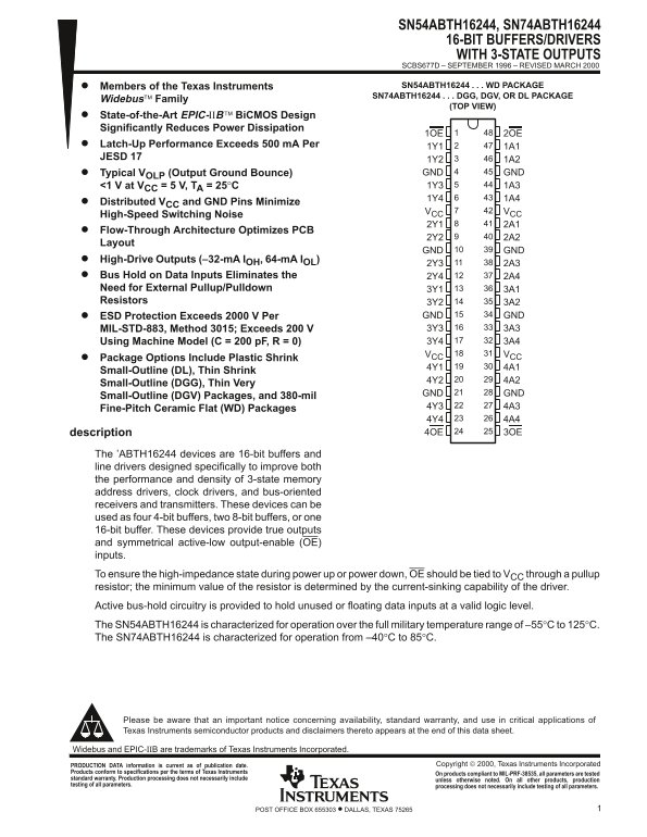
Page 1 Text Content
SN54ABTH16244, SN74ABTH16244
16-BIT BUFFERS/DRIVERS WITH 3-STATE OUTPUTS SCBS677D – SEPTEMBER 1996 – REVISED MARCH 2000 Members of the Texas Instruments SN54ABTH16244 WD PACKAGE
SN74ABTH16244 DGG, DGV, OR DL PACKAGE
Widebus Family
(TOP VIEW)
State-of-the-Art EPIC-ΙΙB Bi CMOS Design Significantly Reduces Power Dissipation
1OE 2OE
Latch-Up Performance Exceeds 500 m A Per 1Y1 1A1 JESD 17
1Y2 1A2 Typical VOLP (Output Ground Bounce) GND GND <1 V at VCC = 5 V, TA = 25°C 1Y3 1A3 1Y4 1A4
Distributed VCC and GND Pins Minimize
VCC VCC
High-Speed Switching Noise
Flow-Through Architecture Optimizes PCB
Layout
GND GND
High-Drive Outputs (–32-m A IOH, 64-m A IOL)
Bus Hold on Data Inputs Eliminates the 2Y4 2A4 Need for External Pullup/Pulldown 3Y1 3A1 Resistors 3Y2 3A2
ESD Protection Exceeds 2000 V Per GND GND MIL-STD-883, Method 3015; Exceeds 200 V 3Y3 3A3 Using Machine Model (C = 200 p F, R = 0) 3Y4 3A4 VCC VCC
Package Options Include Plastic Shrink
Small-Outline (DL), Thin Shrink
Small-Outline (DGG), Thin Very
GND GND
Small-Outline (DGV) Packages, and 380-mil
Fine-Pitch Ceramic Flat (WD) Packages 4Y3 4A3 4Y4 4A4 description 4OE 3OE
The ’ABTH16244 devices are 16-bit buffers and line drivers designed specifically to improve both the performance and density of 3-state memory address drivers, clock drivers, and bus-oriented receivers and transmitters. These devices can be used as four 4-bit buffers, two 8-bit buffers, or one 16-bit buffer. These devices provide true outputs and symmetrical active-low output-enable (OE) inputs. To ensure the high-impedance state during power up or power down, OE should be tied to VCC through a pullup resistor; the minimum value of the resistor is determined by the current-sinking capability of the driver. Active bus-hold circuitry is provided to hold unused or floating data inputs at a valid logic level. The SN54ABTH16244 is characterized for operation over the full military temperature range of –55°C to 125°C. The SN74ABTH16244 is characterized for operation from –40°C to 85°C.
Please be aware that an important notice concerning availability, standard warranty, and use in critical applications of Texas Instruments semiconductor products and disclaimers thereto appears at the end of this data sheet.
Widebus and EPIC-ΙΙB are trademarks of Texas Instruments Incorporated.
Copyright 2000, Texas Instruments Incorporated PRODUCTION DATA information is current as of publication date.
Products conform to specifications per the terms of Texas Instruments On products compliant to MIL-PRF-38535, all parameters are tested standard warranty. Production processing does not necessarily include unless otherwise noted. On all other products, production testing of all parameters. processing does not necessarily include testing of all parameters.
1POST OFFICE BOX 655303 • DALLAS, TEXAS 75265
Page Summary Contents For Texas Instruments SN54ABTH16244, SN74ABTH16244 Data Handbook
Manual Details
| Brand | Texas Instruments |
|---|---|
| Pages | 8 |
| File Size | 106.31 KB |
| Published | June 18, 2026 |
Enter the captcha to get the download link:

Frequently Asked Questions
What is the typical output ground bounce voltage?
The typical output ground bounce is less than <1 V at V = 5 V, T = 25°C.
How should I handle the Output Enable (OE) pins during power cycling?
You must tie OE to V through a pullup resistor to ensure the high-impedance state during power up or down.
What are the temperature limitations for these drivers?
The SN54ABTH16244 is rated for –55°C to 125°C, while the SN74ABTH16244 operates from –40°C to 85°C.
Are these chips suitable for critical industrial applications?
No; they are not designed or warranted for use in life-support devices or other critical applications.