Texas Instruments CY74FCT163244 3660 Owner'\'s Manual, User Guide
Summary
These 16-Bit Buffers/Line Drivers are high-performance CMOS components engineered for demanding, low-power applications such as memory or clock bus interfaces. Featuring advanced "bus hold" input capabilities, they eliminate the need for external pull-up/down resistors and offer enhanced compatibility with modern logic levels. This technical manual covers comprehensive specifications, including robust electrical characteristics, operational diagrams, and guaranteed performance in industrial temperature ranges (–40°C to +85°C).
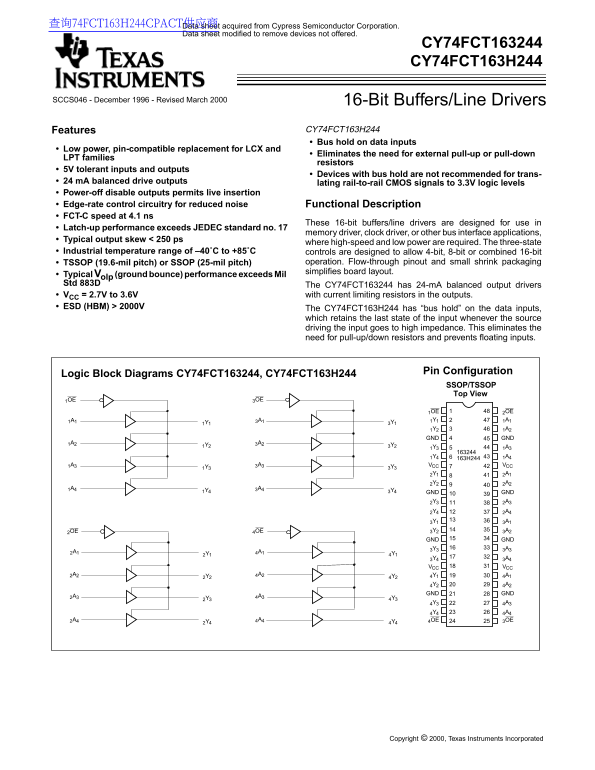
Page 1 Text Content
查询74FCT163H244CPACT供应商 Data sheet acquired from Cypress Semiconductor Corporation.
Data sheet modified to remove devices not offered.
CY74FCT163244 CY74FCT163H244
SCCS046 - December 1996 - Revised March 2000 16-Bit Buffers/Line Drivers
Features CY74FCT163H244 Bus hold on data inputs
Low power, pin-compatible replacement for LCX and
Eliminates the need for external pull-up or pull-down
LPT families
resistors
5V tolerant inputs and outputs
Devices with bus hold are not recommended for trans-
24 m A balanced drive outputs lating rail-to-rail CMOS signals to 3.3V logic levels Power-off disable outputs permits live insertion Edge-rate control circuitry for reduced noise Functional Description FCT-C speed at 4.1 ns
These 16-bit buffers/line drivers are designed for use in
Latch-up performance exceeds JEDEC standard no.
memory driver, clock driver, or other bus interface applications,
Typical output skew < 250 ps
where high-speed and low power are required. The three-state
Industrial temperature range of –40˚C to +85˚C controls are designed to allow 4-bit, 8-bit or combined 16-bit
TSSOP (19.6-mil pitch) or SSOP (25-mil pitch) operation. Flow-through pinout and small shrink packaging simplifies board layout.
Typical Volp (ground bounce) performance exceeds Mil Std 883D The CY74FCT163244 has 24-m A balanced output drivers VCC = 2.7V to 3.6V with current limiting resistors in the outputs. ESD (HBM) > 2000V The CY74FCT163H244 has “bus hold” on the data inputs,
which retains the last state of the input whenever the source driving the input goes to high impedance. This eliminates the need for pull-up/down resistors and prevents floating inputs.
Pin Configuration
Logic Block Diagrams CY74FCT163244, CY74FCT163H244
SSOP/TSSOP Top View
1OE 3OE
1OE 2OE 1A1 3A1 1Y1 1A1
1Y2 1A2 GND GND
1Y3 1A3 1Y4 163H244 1A4 1A3 3A3 VCC VCC
1Y4 3Y4 GND GND
3Y1 3A1 2OE 4OE 3Y2 3A2 GND GND 3Y3 3A3
3Y4 3A4 VCC VCC
GND GND
2A4 4A4 4OE 3OE
Copyright © 2000, Texas Instruments Incorporated
Page Summary Contents For Texas Instruments CY74FCT163244 3660 Owner'\'s Manual, User Guide
Manual Details
| Brand | Texas Instruments |
|---|---|
| Pages | 7 |
| File Size | 61.13 KB |
| Published | June 17, 2026 |
Enter the captcha to get the download link:

Frequently Asked Questions
What is the primary benefit of selecting the model with 'bus hold' input?
The bus hold feature retains the last state of an input even if the source goes to high impedance, which eliminates the need for external pull-up/down resistors.
Are these line drivers compatible with modern board layout practices?
They offer a flow-through pinout and small shrink packaging options like TSSOP or SSOP, simplifying board layout.
What is the required operating temperature range for this device?
The industrial temperature operating range is specified as –40°C to +85°C.
If an input connection point remains unused on the circuit board, how must it be handled?
Unless noted otherwise, unused inputs must always be connected to an appropriate logic voltage level, preferably either VCC or ground.