Texas Instruments SN54AC245, SN74AC245 Owners Manual User Guide
Summary
A datasheet for the SN54AC245 and SN74AC245 octal bus transceivers from Texas Instruments. These devices enable asynchronous two-way communication between data buses with 2V to 6V operation, inputs accepting voltages up to 6V, and maximum propagation delay of 7ns at 5V. The manual covers logic diagram, functional description, absolute maximum ratings, electrical characteristics, switching characteristics, and package information for PDIP, SOIC, SSOP, TSSOP, CDIP, CFP, and LCCC variants. Targeted at digital design engineers and system architects building bus interface and data communication circuits.
Page 1 Text Content
SCAS461F − FEBRUARY 1995 − REVISED OCTOBER 2003
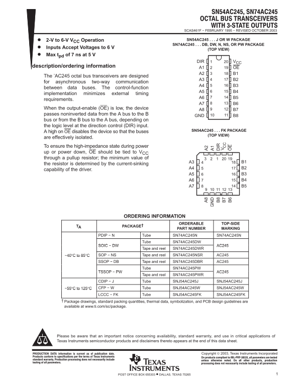
2-V to 6-V VCC Operation SN54AC245 J OR W PACKAGE SN74AC245 DB, DW, N, NS, OR PW PACKAGE
Inputs Accept Voltages to 6 V
(TOP VIEW)
Max tpd of 7 ns at 5 V
DIR VCC
description/ordering information
A1 OE A2 B1
The ’AC245 octal bus transceivers are designed
for asynchronous two-way communication
between data buses. The control-function
implementation minimizes external timing
requirements.
When the output-enable (OE) is low, the device
passes noninverted data from the A bus to the B
GND B8
bus or from the B bus to the A bus, depending on the logic level at the direction control (DIR) input.
SN54AC245 FK PACKAGE
A high on OE disables the device so that the buses
(TOP VIEW)
are effectively isolated. To ensure the high-impedance state during power up or power down, OE should be tied to VCC through a pullup resistor; the minimum value of
the resistor is determined by the current-sinking
capability of the driver.
ORDERING INFORMATION
ORDERABLE TOP-SIDE
TA PACKAGE†
PART NUMBER MARKING
PDIP − N Tube SN74AC245N SN74AC245N
Tube SN74AC245DW
SOIC − DW AC245
Tape and reel SN74AC245DWR
−40°C to 85°C SOP − NS Tape and reel SN74AC245NSR AC245 SSOP − DB Tape and reel SN74AC245DBR AC245
Tube SN74AC245PW
TSSOP − PW AC245
Tape and reel SN74AC245PWR
CDIP − J Tube SNJ54AC245J SNJ54AC245J −55°C to 125°C CFP − W Tube SNJ54AC245W SNJ54AC245W LCCC − FK Tube SNJ54AC245FK SNJ54AC245FK
Package drawings, standard packing quantities, thermal data, symbolization, and PCB design guidelines are available at www.ti.com/sc/package.
Please be aware that an important notice concerning availability, standard warranty, and use in critical applications of Texas Instruments semiconductor products and disclaimers thereto appears at the end of this data sheet.
1POST OFFICE BOX 655303 • DALLAS, TEXAS 75265
Page Summary Contents For Texas Instruments SN54AC245, SN74AC245 Owners Manual User Guide
Manual Details
| Brand | Texas Instruments |
|---|---|
| Pages | 16 |
| File Size | 537.95 KB |
| Published | June 16, 2026 |
Enter the captcha to get the download link:

Frequently Asked Questions
How do I ensure the SN74AC245 enters a high-impedance state during power up/down?
Connect the OE (output enable) pin to VCC through a pullup resistor to ensure a high-impedance state.
What is the direction control logic for the SN74AC245 octal bus transceiver?
When OE is low, DIR low sends data from bus B to A, and DIR high sends data from bus A to B.
What is the recommended operating voltage range for the SN74AC245?
The device operates from 2V to 6V VCC.
What is the maximum propagation delay of the SN74AC245?
The maximum tpd is 7 ns at 5V.
What package options are available for the SN74AC245?
It is available in DB, DW, N, NS, and PW packages.