Texas Instruments CDCV857B, CDCV857BI Data Handbook / Specifications Guide
Summary
The CDCV857B is a high-performance, low-jitter clock buffer and differential signal driver designed to distribute a single input clock to ten reliable output pairs. Featuring ultra-low skew and advanced power management, this module ensures optimal stability across frequencies ranging from 60 MHz to 200 MHz. The comprehensive manual outlines its crystal-clear operation, detailing technical specifications, functional block diagrams, pin configurations, and low-power modes for electrical engineers developing complex digital systems requiring precise clock distribution solutions.
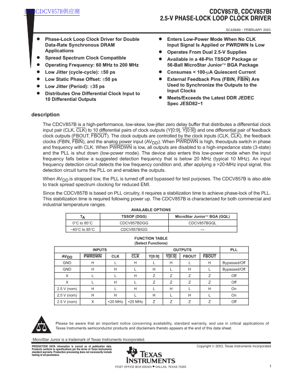
Page 1 Text Content
查询CDCV857B供应商
SCAS689 − FEBRUARY 2003
Phase-Lock Loop Clock Driver for Double Enters Low-Power Mode When No CLK Data-Rate Synchronous DRAM Input Signal Is Applied or PWRDWN Is Low Applications
Operates From Dual 2.5-V Supplies
Spread Spectrum Clock Compatible
Available in a 48-Pin TSSOP Package or Operating Frequency: 60 MHz to 200 MHz 56-Ball Micro Star Junior BGA Package
Low Jitter (cycle-cycle): ±50 ps Consumes < 100-µA Quiescent Current Low Static Phase Offset: ±50 ps External Feedback Pins (FBIN, FBIN) Are
Used to Synchronize the Outputs to the
Low Jitter (Period): ±35 ps
Input Clocks
Distributes One Differential Clock Input to
Meets/Exceeds the Latest DDR JEDEC
10 Differential Outputs
Spec JESD82−1
description The CDCV857B is a high-performance, low-skew, low-jitter zero delay buffer that distributes a differential clock input pair (CLK, CLK) to 10 differential pairs of clock outputs (Y[0:9], Y[0:9]) and one differential pair of feedback clock outputs (FBOUT, FBOUT). The clock outputs are controlled by the clock inputs (CLK, CLK), the feedback clocks (FBIN, FBIN), and the analog power input (AVDD). When PWRDWN is high, theoutputs switch in phase and frequency with CLK. When PWRDWN is low, all outputs are disabled to a high-impedance state (3-state) and the PLL is shut down (low-power mode). The device also enters this low-power mode when the input frequency falls below a suggested detection frequency that is below 20 MHz (typical 10 MHz). An input frequency detection circuit detects the low frequency condition and, after applying a >20-MHz input signal, this detection circuit turns the PLL on and enables the outputs. When AVDD is strapped low, the PLL is turned off and bypassed for test purposes. The CDCV857B is also able to track spread spectrum clocking for reduced EMI. Since the CDCV857B is based on PLL circuitry, it requires a stabilization time to achieve phase-lock of the PLL. This stabilization time is required following power up. The CDCV857B is characterized for both commercial and industrial temperature ranges.
AVAILABLE OPTIONS
TA TSSOP (DGG) Micro Star Junior BGA (GQL) 0°C to 85°C CDCV857BDGG CDCV857BGQL −40°C to 85°C CDCV857BIGG
FUNCTION TABLE (Select Functions)
INPUTS OUTPUTS PLL
AVDD PWRDWN CLK CLK Y[0:9] Y[0:9] FBOUT FBOUT GND Bypassed/Off GND Bypassed/Off
Off Off
2.5 V (nom) On 2.5 V (nom) On 2.5 V (nom) <20 MHz <20 MHz Off
Please be aware that an important notice concerning availability, standard warranty, and use in critical applications of Texas Instruments semiconductor products and disclaimers thereto appears at the end of this data sheet.
Micro Star Junior is a trademark of Texas Instruments Incorporated.
1POST OFFICE BOX 655303 • DALLAS, TEXAS 75265
Page Summary Contents For Texas Instruments CDCV857B, CDCV857BI Data Handbook / Specifications Guide
Manual Details
| Brand | Texas Instruments |
|---|---|
| Pages | 14 |
| File Size | 269.22 KB |
| Published | June 02, 2026 |
Enter the captcha to get the download link:

Frequently Asked Questions
What are the primary outputs distributed by the CDCV857B?
It distributes one differential clock input pair (CLK, CLK) to 10 differential pairs of clock outputs (Y[0:9]) and one feedback output pair (FBOUT, FBOUT).
How can I enter a low-power or disabled state?
Setting PWRDWN low disables all outputs to a high-impedance state, shutting down the PLL. Alternatively, it enters this mode if the input frequency falls below 20 MHz.
Is there a required time after power-up?
Yes, since the CDCV857B utilizes PLL circuitry, it requires a mandatory stabilization time following initial power up to achieve phase-lock.