Texas Instruments CD54ACT20, CD74ACT20 Data Handbook/Manual
Summary
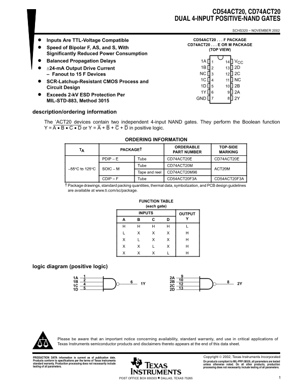
Texas Instruments CD54ACT20/CD74ACT20 dual 4-input NAND gate with TTL-compatible inputs, bipolar speed, low CMOS power, 24mA output drive, fanout to 15 devices, SCR-latchup resistance, and 2kV ESD protection. Available in PDIP, SOIC, and CDIP packages. For digital logic designers in industrial, military, and commercial electronic circuits.
Page 1 Text Content
CD54ACT20, CD74ACT20
DUAL 4-INPUT POSITIVE-NAND GATES
SCHS320 – NOVEMBER 2002
Inputs Are TTL-Voltage Compatible CD54ACT20 F PACKAGE CD74ACT20 E OR M PACKAGE
Speed of Bipolar F, AS, and S, With
(TOP VIEW)
Significantly Reduced Power Consumption Balanced Propagation Delays 1A VCC
±24-m A Output Drive Current 1B 2D – Fanout to 15 F Devices NC 2C 1C NC
SCR-Latchup-Resistant CMOS Process and
Circuit Design
Exceeds 2-k V ESD Protection Per
GND 2Y
MIL-STD-883, Method 3015
description/ordering information The ’ACT20 devices contain two independent 4-input NAND gates. They perform the Boolean function Y = A • B • C • D or Y = A + B + C + D in positive logic.
ORDERING INFORMATION
ORDERABLE TOP-SIDE
TA PACKAGE†
PART NUMBER MARKING
PDIP – E Tube CD74ACT20E CD74ACT20E
Tube CD74ACT20M
55°C to 125°C SOIC ACT20M–
Tape and reel CD74ACT20M96
CDIP – F Tube CD54ACT20F3A CD54ACT20F3A
Package drawings, standard packing quantities, thermal data, symbolization, and PCB design guidelines are available at www.ti.com/sc/package.
FUNCTION TABLE (each gate) INPUTS OUTPUT
logic diagram (positive logic)
Please be aware that an important notice concerning availability, standard warranty, and use in critical applications of Texas Instruments semiconductor products and disclaimers thereto appears at the end of this data sheet.
PRODUCTION DATA information is current as of publication date. Copyright 2002, Texas Instruments Incorporated
Products conform to specifications per the terms of Texas Instruments On products compliant to MIL-PRF-38535, all parameters are tested standard warranty. Production processing does not necessarily include unless otherwise noted. On all other products, production testing of all parameters. processing does not necessarily include testing of all parameters.
1POST OFFICE BOX 655303 • DALLAS, TEXAS 75265
Page Summary Contents For Texas Instruments CD54ACT20, CD74ACT20 Data Handbook/Manual
Manual Details
| Brand | Texas Instruments |
|---|---|
| Pages | 11 |
| File Size | 482.71 KB |
| Published | June 17, 2026 |
Enter the captcha to get the download link:

Frequently Asked Questions
What logic function do the ACT20 devices perform?
They perform Y = A • B • C • D or Y = A + B + C + D in positive logic via two 4-input NAND gates.
What is the output drive current of these gates?
They have ±24-mA output drive current, with fanout to 15 F devices.
What supply voltage range is recommended for operation?
The recommended supply voltage VCC is 4.5 V to 5.5 V.
How should unused inputs be handled?
All unused inputs must be held at VCC or GND to ensure proper device operation.