# A B C D E F G H I J K L M N O P Q R S T U V W X Y Z

SHARP LZ21N3 User Manual and Data Sheet

Summary

The LZ21N3 is a high-precision, 1/2-type solid-state CCD image sensor ideal for advanced vision systems requiring stable, high-resolution color imaging across an 8.08 mm format. This comprehensive manual provides engineers and developers with essential technical specifications, including detailed pin connections, absolute maximum ratings, recommended electrical operating conditions, and deep characteristics analysis (PNRU, DSNU). It serves as a critical resource for proper integration, ensuring users can maximize sensor performance while adhering to strict handling precautions for reliable industrial and scientific applications.
📄 Preview PAGE OF 19

Page 1 Text Content

查询LZ21N3供应商 LZ21N3

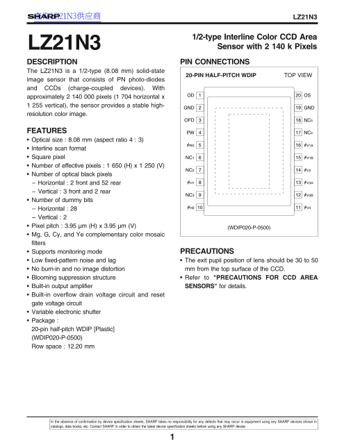
1/2-type Interline Color CCD Area LZ21N3 Sensor with 2 140 k Pixels

DESCRIPTION PIN CONNECTIONS The LZ21N3 is a 1/2-type (8.08 mm) solid-state

20-PIN HALF-PITCH WDIP TOP VIEW

image sensor that consists of PN photo-diodes and CCDs (charge-coupled devices). With

1OD OS

approximately 2 140 000 pixels (1 704 horizontal x 1 255 vertical), the sensor provides a stable high-

2GND GND

resolution color image.

3OFD NC5

FEATURES 4PW NC4 Optical size : 8.08 mm (aspect ratio 4 : 3)

5ØRS ØV1A

Interline scan format Square pixel 6NC1 ØV1B Number of effective pixels : 1 650 (H) x 1 250 (V)

7NC2 ØV2

Number of optical black pixels

Horizontal : 2 front and 52 rear 8ØH1 ØV3A

Vertical : 3 front and 2 rear

9NC3 ØV3B

Number of dummy bits

Horizontal : 28 Vertical : 2 Pixel pitch : 3.95 µm (H) x 3.95 µm (V)

(WDIP020-P-0500)

Mg, G, Cy, and Ye complementary color mosaic filters Supports monitoring mode PRECAUTIONS Low fixed-pattern noise and lag The exit pupil position of lens should be 30 to 50 No burn-in and no image distortion mm from the top surface of the CCD. Blooming suppression structure Refer to "PRECAUTIONS FOR CCD AREA Built-in output amplifier SENSORS" for details. Built-in overflow drain voltage circuit and reset gate voltage circuit Variable electronic shutter Package : 20-pin half-pitch WDIP [Plastic] (WDIP020-P-0500) Row space : 12.20 mm

In the absence of confirmation by device specification sheets, SHARP takes no responsibility for any defects that may occur in equipment using any SHARP devices shown in catalogs, data books, etc. Contact SHARP in order to obtain the latest device specification sheets before using any SHARP device.

Page Summary Contents For SHARP LZ21N3 User Manual and Data Sheet

Page 1 查询LZ21N3供应商 LZ21N3 1/2-type Interline Color CCD Area LZ21N3 Sensor with 2 140 k Pixels DESCRIPTION PIN CONNECTIONS The LZ21N3 is a 1/2-type (8.08 mm) solid-state 20-PIN HALF-PITCH WDIP TOP VIEW image ...
Page 2 LZ21N3 PIN DESCRIPTION SYMBOL PIN NAME OD Output transistor drain OS Output signals ØRS Reset transistor clock ØV1A, ØV1B, ØV2, ØV3A, ØV3B, ØV4 Vertical shift register clock ØH1, ØH2 Horizontal shift ...
Page 3 LZ21N3 RECOMMENDED OPERATING CONDITIONS PARAMETER SYMBOL MIN. TYP. MAX. UNIT NOTE Ambient operating temperature TOPR 25.0 ˚C Output transistor drain voltage VOD 12.5 13.0 13.5 p-p level 1V20.919.518.6...
Page 4 LZ21N3 CHARACTERISTICS (Drive method : 1/30 s frame accumulation) (TA = +25 ˚C, Operating conditions : The typical values specified in "RECOMMENDED OPERATING CONDITIONS". Color temperature o...
Page 5 LZ21N3 PIXEL STRUCTURE OPTICAL BLACK (2 PIXELS) OPTICAL BLACK OPTICAL BLACK (2 PIXELS) (52 PIXELS) 1 pin OPTICAL BLACK (3 PIXELS) COLOR FILTER ARRAY Pin arrangement ØV3B Ye Cy Ye Cy Ye Cy Ye Cy Ye Cy ...
Page 6 LZ21N3 TIMING CHART TIMING CHART EXAMPLE Pulse diagram in more detail is shown in figures q to t after the next page. Field accumulation mode Frame accumulation Frame accumulation mode Field accumulat...
Page 7 LZ21N3 q VERTICAL TRANSFER TIMING ¿FIELD ACCUMULATION MODE¡ Shutter speed 1/30 s OS Ye Cy GMg Ye Cy GMg Ye Cy GMg Ye Cy GMg Ye Cy GMg Ye Cy GMg Ye Cy GMg Ye Cy q' VERTICAL TRANSFER TIMING ¿FIELD ACCUM...
Page 8 LZ21N3 w VERTICAL TRANSFER TIMING ¿FRAME ACCUMULATION MODE AT FIRST¡ Shutter speed 1/15 s OS Ye Cy GMg GMg Ye Cy GMg Ye Cy GMg Ye Cy GMg Ye Cy GMg Ye Cy Not for use * Do not use the frame signals imme...
Page 9 LZ21N3 r VERTICAL TRANSFER TIMING ¿FRAME ACCUMULATION MODE¡ Charge swept transfer (684 stages) OB1 OB1 OB3 OS GMg GMg GMg GMg Ye Cy Ye Cy GMg Not for use t VERTICAL TRANSFER TIMING ¿FIELD ACCUMULATION...
Page 10 LZ21N3 READOUT TIMING ¿FIELD ACCUMULATION MODE¡ 6.7 µs 40.9 µs (732 bits) (120 bits) 6.7 µs 58.8 µs (1 052 bits) (120 bits) * Keep over 2.2 µs when vertical transfer clock pulse is overlapping. READOU...
Page 11 LZ21N3 HORIZONTAL TRANSFER TIMING ¿FIELD ACCUMULATION MODE¡-1 1 clk = 55.8 ns (= 1/17.9 MHz) πππ1650 OB (52) 40 clk (= 2.2 µs) Double transfer ØV1A ØV1B Triple transfer ØV1A ØV1B
Page 12 LZ21N3 HORIZONTAL TRANSFER TIMING ¿FIELD ACCUMULATION MODE¡-2 1 clk = 55.8 ns (= 1/17.9 MHz) PRE SCAN (28) OB (2) OUTPUT (1 650) 1πππππππ Double transfer Triple transfer ØV1A ØV1B
Page 13 LZ21N3 HORIZONTAL TRANSFER TIMING ¿FRAME ACCUMULATION MODE¡-1 1 clk = 55.8 ns (= 1/17.9 MHz) OS ..1650 OB (52) 40 clk (= 2.2 µs) Standard transfer
Page 14 LZ21N3 HORIZONTAL TRANSFER TIMING ¿FRAME ACCUMULATION MODE¡-2 1 clk = 55.8 ns (= 1/17.9 MHz) HD ØH1 PRE SCAN (28) OB (2) OUTPUT (1 650) 1πππππππ Standard transfer
Page 15 LZ21N3 CHARGE SWEPT TRANSFER TIMING ¿e¡ * Keep over 1.1 µs when vertical transfer clock pulse of charge swept transfer is overlapping. CHARGE SWEPT TRANSFER TIMING ¿r¡ * Keep over 1.1 µs when vertical...
Page 16 LZ21N3 SYSTEM CONFIGURATION EXAMPLE OD OS GND GND OFD NC5 PW NC4 ØV1AØRS NC1 ØV1B NC2 ØV2 NC3 ØV3B LR LZ 3(* POFD VOFDH 3A VMb VH3BX VL OFDX 1) S, FD NC VH1AX se th ci rc ui t p ar am et er in di ca t...
Page 17 PACKAGES FOR CCD AND CMOS DEVICES PACKAGE (Unit : mm) 20 WDIP (WDIP020-P-0500) Center of effective imaging area and center of package Rotation error of die : ¬ = 1.0˚MAX. CCD (◊ 1 : Effective imaging ...
Page 18 PRECAUTIONS FOR CCD AREA SENSORS PRECAUTIONS FOR CCD AREA SENSORS (In the case of plastic packages) 1. Package Breakage The leads of the package are fixed with In order to prevent the package from bei...
Page 19 PRECAUTIONS FOR CCD AREA SENSORS 3) To avoid generating static electricity, The contamination on the glass surface a. do not scrub the glass surface with cloth or should be wiped off with a clean appl...

Manual Details

Brand Sharp
Pages 19
File Size 159.48 KB
Published June 02, 2026
71 views

Enter the captcha to get the download link:

captcha

Frequently Asked Questions

What is the optical size and pixel count of the LZ21N3 sensor?

The optical size is 8.08 mm (4:3 aspect ratio), with an effective pixel count of 1,650 (H) x 1,250 (V).

What are the operating temperature ranges for this device?

The storage temperature range is -40 to +85°C, while the ambient operating temperature range is -20 to +70°C.

How should I clean or handle the CCD surface?

Handle the CCD in a class 100 or cleaner environment, and only wipe dust with an ionized air blower or specialized applicator, never scrubbing.