# A B C D E F G H I J K L M N O P Q R S T U V W X Y Z

ROHM BU2394KN BU2396 Digital Camera User Manuals and Data Sheets

Summary

These high-performance integrated circuit chips are professional clock generators designed to provide three essential output types—CCD, USB, and VIDEO clocks—for sophisticated digital still and video cameras. Built with compact VQFN packaging, they simplify system architecture by consolidating multiple clock functions into a powerful single chip. This manual details the technical specifications for integrating these low-jitter generators into mobile camera equipment, ensuring reliable performance with simplified power and component counts.
📄 Preview PAGE OF 17

Page 1 Text Content

TECHNICAL NOTE

High-performance Clock Generator Series

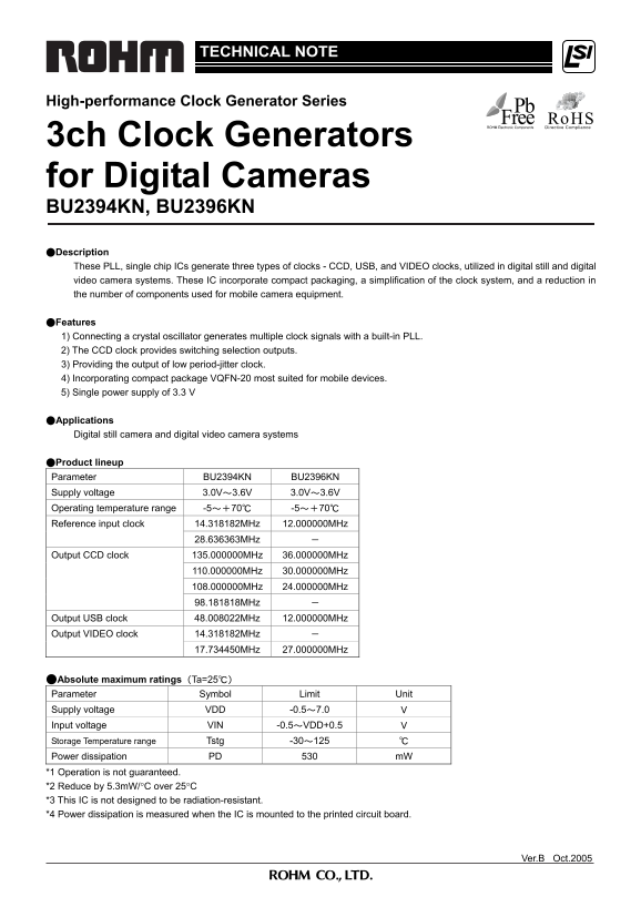
3ch Clock Generators for Digital Cameras BU2394KN, BU2396KN ●Description These PLL, single chip ICs generate three types of clocks - CCD, USB, and VIDEO clocks, utilized in digital still and digital video camera systems. These IC incorporate compact packaging, a simplification of the clock system, and a reduction in the number of components used for mobile camera equipment. ●Features 1) Connecting a crystal oscillator generates multiple clock signals with a built-in PLL. 2) The CCD clock provides switching selection outputs. 3) Providing the output of low period-jitter clock. 4) Incorporating compact package VQFN-20 most suited for mobile devices. 5) Single power supply of 3.3 V ●Applications Digital still camera and digital video camera systems

●Product lineup Parameter BU2394KN BU2396KN Supply voltage 3.0V~3.6V 3.0V~3.6V Operating temperature range -5~+70℃ -5~+70℃

14.318182MHz 12.000000MHz Reference input clock 28.636363MHz -

Output CCD clock 135.000000MHz 36.000000MHz

110.000000MHz 30.000000MHz 108.000000MHz 24.000000MHz 98.181818MHz -

Output USB clock 48.008022MHz 12.000000MHz

14.318182MHz - Output VIDEO clock 17.734450MHz 27.000000MHz

●Absolute maximum ratings(Ta=25℃) Parameter Symbol Limit Unit Supply voltage VDD -0.5~7.0 V Input voltage VIN -0.5~VDD+0.5 V Storage Temperature range Tstg -30~125 ℃ Power dissipation PD 530 m W *1 Operation is not guaranteed. *2 Reduce by 5.3m W/°C over 25°C *3 This IC is not designed to be radiation-resistant. *4 Power dissipation is measured when the IC is mounted to the printed circuit board.

Ver.B Oct.2005

Page Summary Contents For ROHM BU2394KN BU2396 Digital Camera User Manuals and Data Sheets

Page 1 TECHNICAL NOTE High-performance Clock Generator Series 3ch Clock Generators for Digital Cameras BU2394KN, BU2396KN ●Description These PLL, single chip ICs generate three types of clocks - CCD, USB, an...
Page 2 ●Recommended operating range Parameter Symbol Limit Unit Supply voltage VDD 3.0~3.6 V Input H voltage VINH 0.8VDD~VDD V Input L voltage VINL 0.0~0.2VDD V Operating temperature Topr -5~+70 ℃ Output loa...
Page 3 BU2396N(VDD=3.3V, Ta=25℃, Crystal =12.000000MHz, unless otherwise specified.) Limit Parameter Symbol Unit Condition Min. Typ. Max. 【Action circuit current】 IDD - 23 35 m A At no load 【Output H voltage...
Page 4 ●Reference data (BU2394KN basic data) 1. 0V di 1. 0V di 1. 0V di 1. 0V di RBW=1KHz VBW=100Hz 1.0nsec/div 500psec/div 10KHz/div Fig.1 135MHz output wave Fig.2 135MHz Period-Jitter Fig.3 135MHz Spectrum...
Page 5 ●Reference data (BU2394KN basic data) 1. 0V di 1. 0V di 1. 0V di RBW=1KHz VBW=100Hz 5.0nsec/div 500psec/div 10KHz/div Fig.13 48MHz output wave Fig.14 48MHz Period-Jitter Fig.15 48MHz Spectrum At VDD=3...
Page 6 ●Reference data (BU2394KN Temperature and Supply voltage variations data) ut y: ut y[ ut y: ut y[ ut y: ut y[ ut y: ut y[ VDD=2.9V VDD=2.9V VDD=2.9V VDD=3.3V VDD=3.3V VDD=3.3V VDD=3.7V VDD=3.7V VDD=3....
Page 7 ●Reference data (BU2394KN Temperature and Supply voltage variations data) ID ID [m A] ut y: ut y[ ut y: ut y[ ut y: ut y[ VDD=3.7V VDD=3.3V VDD=3.7V VDD=2.9V VDD=3.3V VDD=2.9V VDD=2.9V VDD=3.3V VDD=3....
Page 8 ●Reference data (BU2396KN basic data) 1. 0V di 1. 0V di 1. 0V di 1. 0V di RBW=1KHz VBW=100Hz 5.0nsec/div 500psec/div 10KHz/div Fig.44 36MHz output waveform Fig.45 136MHz Period-Jitter Fig.46 36MHz Spe...
Page 9 ●Reference data (BU2396KN basic data) ut y: ut y[ ut y: ut y[ ut y: ut y[ 1. 0V di RBW=1KHz VBW=100Hz 5.0nsec/div 500psec/div 10KHz/div Fig.56 12MHz output waveform Fig.57 12MHz Period-Jitter Fig.58 1...
Page 10 ●Reference data (BU2396KN Temperature and Supply voltage variations data) ID ID [m ut y: ut y[ ut y: ut y[ VDD=2.9V VDD=3.3V VDD=3.7V VDD=3.7V VDD=3.7V VDD=3.3V VDD=3.3V VDD=2.9V VDD=2.9V Temperature:...
Page 11 ●BU2396KN Operation Modes When XTAL_SEL=L, (When a crystal oscillator of 14.318182-MHz frequency is used) Xtal(MHz) CLK2ON FS1 FS2 FS3 CLK1(MHz) CLK2(MHz) REF_CLK(MHz) 14.318182 L H H H 135.000000 Fix...
Page 12 ●BU2396KN Operation Modes VCLK UCLK PLL1 PLL2 TGCLK_SEL1 TGCLK_SEL2 TGCLK_EN VCLK_EN TGCLK_PD VCLK_PD TGCLK Output Output Output 30M,24M 36M,27M 0 Fixed to L Power-Down Power-Down Fixed to L Normal op...
Page 13 ●BU2394KN Application Circuit / Description of Terminal for Video 14.318182MHz 0.1u F 17.734450MHz for USB 135.000000MHz 48.008022MHz 108.000000MHz TE T1 110.000000MHz 98.181818MHz CLK1 7: TA L_ _C 1:...
Page 14 ●BU2396KN Application Circuit / Description of Terminal XTAL OSCXOUT 12.000000MHz UCLK for Video 27.000000MHz 0.1u F TGCLK_EN for USB 6: TE LK _P 12.000000MHz TGCLK_SEL2 DATA 7: TG LK _S L2 LK 30.0000...
Page 15 ●Cautions on Use 1. Absolute Maximum Ratings An excess in the absolute maximum ratings, such as supply voltage , temperature range of operating conditions, etc., can break down devices, thus making im...
Page 16 ●Selection of order type Type 23946 Part No. Package Type Packing specification KN:VQFN E2: Reel-like emboss taping 0. 4. 2± 0. 6 EB U 2 3 9 K Part No. Type 2396 Package Type Packing specification KN:...
Page 17 Appendix Notes No technical content pages of this document may be reproduced in any form or transmitted by any means without prior permission of ROHM CO.,LTD. The contents described herein are subject...

Manual Details

Brand ROHM
Pages 17
File Size 880.78 KB
Published May 27, 2026
81 views

Enter the captcha to get the download link:

captcha

Frequently Asked Questions

What types of clocks does this IC generate for camera systems?

It generates three types: CCD, USB, and VIDEO clocks.

What is the recommended operating voltage range?

The specified operating voltage supply (VDD) range is 3.0V to 3.6V.

Does the component assist with simplifying camera system design?

Yes, it incorporates compact packaging and simplifies the clock system by reducing necessary components for mobile equipment.

Are these chips suitable for life-critical equipment like medical or aerospace devices?

No; users must consult sales representatives if intended for high-reliability applications and are advised to implement fail-safe measures.