Panasonic 2SC1383, 2SC1384 Owner's Manual and User Guide
Summary
These reliable 2SC1383/2SC1384 transistors are a complementary pair designed specifically for low-frequency power and driver amplification circuits. This technical documentation provides engineers and designers with comprehensive electrical datasheets, including critical specifications like saturation voltages (VCE(sat), VBE(sat)), transition frequencies, and performance curves across varying operating temperatures. Ideal for professional electronics applications requiring stable and dependable switching or amplification components.
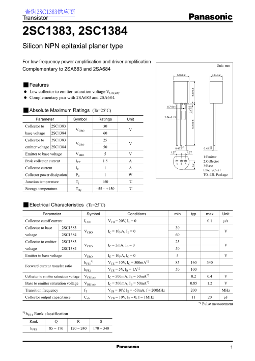
Page 1 Text Content
查询2SC1383供应商 Transistor
2SC1383, 2SC1384 Silicon NPN epitaxial planer type For low-frequency power amplification and driver amplification
Unit: mm
Complementary to 2SA683 and 2SA684
Features Low collector to emitter saturation voltage VCE(sat). Complementary pair with 2SA683 and 2SA684.
Absolute Maximum Ratings (Ta=25˚C)
Parameter Symbol Ratings Unit Collector to 2SC1383
base voltage 2SC1384 Collector to 2SC1383
emitter voltage 2SC1384 +0.2 +0.2 0.45 –0.1 0.45 –0.1 1.271.27
Emitter to base voltage VEBO
1:Emitter
Peak collector current ICP 1.5 2:Collector
3:Base
Collector current IC
EIAJ:SC–51 Collector power dissipation PC TO–92L Package
Junction temperature Tj ˚C Storage temperature Tstg –55 ~ +150 ˚C 0.
Electrical Characteristics (Ta=25˚C) Parameter Symbol Conditions min typ max Unit Collector cutoff current ICBO VCB = 20V, IE = 0 0.1 µA
Collector to base 2SC1383
VCBO IC = 10µA, IE = 0
voltage 2SC1384
Collector to emitter 2SC1383
VCEO IC = 2m A, IB = 0
voltage 2SC1384 Emitter to base voltage VEBO IE = 10µA, IC = 0
*1 h FE1 VCE = 10V, IC = 500m A*2
Forward current transfer ratio
h FE2 VCE = 5V, IB = 1A*2
Collector to emitter saturation voltage VCE(sat) IC = 500m A, IB = 50m A*2 0.2 0.4 Base to emitter saturation voltage VBE(sat) IC = 500m A, IB = 50m A*2 0.85 1.2 Transition frequency f T VCB = 10V, IE = –50m A, f = 200MHz MHz Collector output capacitance Cob VCB = 10V, IE = 0, f = 1MHz p F
*2 Pulse measurement
*1h FE1 Rank classification
Rank h FE1 85 ~ 170 120 ~ 240 170 ~ 340
Page Summary Contents For Panasonic 2SC1383, 2SC1384 Owner's Manual and User Guide
Manual Details
| Brand | Panasonic |
|---|---|
| Pages | 3 |
| File Size | 35.81 KB |
| Published | June 04, 2026 |
Enter the captcha to get the download link:

Frequently Asked Questions
What is the maximum collector power dissipation for this pair of transistors?
The maximum rated collector power dissipation (Pc) is 1W.
Are these transistors suitable for high-frequency applications?
Their transition frequency (fT) ranges from 200 MHz to 340 MHz, making them viable for RF boosting and driver amplification.
What are the recommended operating temperatures for use?
The specified junction temperature range (Tj) is 150˚C, with storage temperature ranging from –55°C to +150°C.
How does this pair perform under different ambient temperatures?
At 75˚C ambient temperature, the optimal operational parameters are listed in the detailed derating curves provided in the specifications.