National Semiconductor LP5900 Specifications and User Guide
Summary
The LP5900 is an ultra-low noise, 150 mA linear regulator designed for sophisticated RF and analog circuits. This high-performance component guarantees stable power delivery with industry-leading noise figures and requires no external bypass capacitor—simplifying circuit design. The manual provides extensive technical specifications, covering multiple output voltages (up to 3.3V), various package options (micro SMD/LLP), detailed application circuit configurations, and suitability for demanding applications like cellular phones and wireless LAN devices.
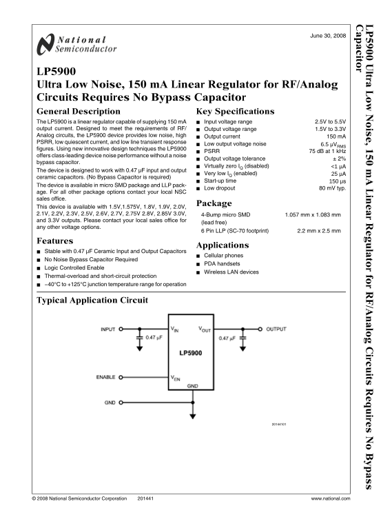
Page 1 Text Content
ltra is , 1 in r R la to r fo r R /A lo irc its ire ito
June 30, 2008
LP5900 Ultra Low Noise, 150 m A Linear Regulator for RF/Analog Circuits Requires No Bypass Capacitor General Description Key Specifications
The LP5900 is a linear regulator capable of supplying 150 m A Input voltage range 2.5V to 5.5V
output current. Designed to meet the requirements of RF/ Output voltage range 1.5V to 3.3V Analog circuits, the LP5900 device provides low noise, high Output current 150 m A PSRR, low quiescent current, and low line transient response
Low output voltage noise 6.5 μVRMS
figures. Using new innovative design techniques the LP5900
PSRR 75 d B at 1 k Hz
offers class-leading device noise performance without a noise
Output voltage tolerance ± 2%
bypass capacitor.
Virtually zero IQ (disabled) <1 μA
The device is designed to work with 0.47 μF input and output
Very low IQ (enabled) 25 μA
ceramic capacitors. (No Bypass Capacitor is required)
Start-up time 150 μs
The device is available in micro SMD package and LLP pack-
Low dropout 80 m V typ.
age. For all other package options contact your local NSC sales office.
Package
This device is available with 1.5V,1.575V, 1.8V, 1.9V, 2.0V, 2.1V, 2.2V, 2.3V, 2.5V, 2.6V, 2.7V, 2.75V 2.8V, 2.85V 3.0V, 4-Bump micro SMD 1.057 mm x 1.083 mm and 3.3V outputs. Please contact your local sales office for
(lead free)
any other voltage options.
6 Pin LLP (SC-70 footprint) 2.2 mm x 2.5 mm
Features
Applications
Stable with 0.47 μF Ceramic Input and Output Capacitors
Cellular phones
No Noise Bypass Capacitor Required
PDA handsets
Logic Controlled Enable
Wireless LAN devices
Thermal-overload and short-circuit protection −40°C to +125°C junction temperature range for operation
Typical Application Circuit
© 2008 National Semiconductor Corporation www.national.com
Page Summary Contents For National Semiconductor LP5900 Specifications and User Guide
Manual Details
| Brand | National |
|---|---|
| Pages | 12 |
| File Size | 305.88 KB |
| Published | June 04, 2026 |
Enter the captcha to get the download link:

Frequently Asked Questions
Is a bypass capacitor necessary for this regulator?
No Bypass Capacitor is required, allowing users to simplify circuit design.
What are the electrical specifications of the LP5900?
It supplies up to 150 mA and accepts an input voltage range between 2.5V and 5.5V.
What is the device's operational temperature range?
The junction temperature range for operation is specified from -40°C to +125°C.