National Semiconductor DS90C383B User's Manual and Specifications
Summary
This programmable LVDS transmitter is engineered for reliable, high-speed data links in Flat Panel Display (FPD) applications, supporting standards like VGA and XGA up to 1.8 Gbps. The advanced chip design minimizes EMI while significantly reducing cable size and power consumption compared to traditional interfaces. This manual provides comprehensive technical specifications, detailed electrical characteristics, and operational guides for system designers integrating the DS90C383B into their high-bandwidth display solutions.
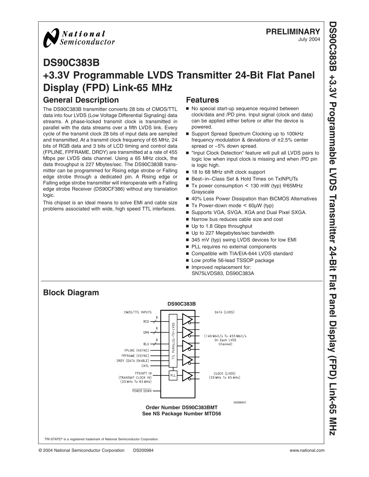
Page 1 Text Content
PRELIMINARY
90C 383B +3.3V rogram able LV Transm itter 24-B it Flat anel D isplay (FP Link-65
DS90C383B +3.3V Programmable LVDS Transmitter 24-Bit Flat Panel Display (FPD) Link-65 MHz General Description Features
The DS90C383B transmitter converts bits of CMOS/TTL No special start-up sequence required between data into four LVDS (Low Voltage Differential Signaling) data clock/data and /PD pins. Input signal (clock and data) streams. phase-locked transmit clock is transmitted in can be applied either before or after the device is parallel with the data streams over fifth LVDS link. Every powered. cycle of the transmit clock bits of input data are sampled Support Spread Spectrum Clocking up to 100k Hz
and transmitted. At transmit clock frequency of MHz, frequency modulation deviations of ±2.5% center
bits of RGB data and bits of LCD timing and control data spread or −5% down spread.
(FPLINE, FPFRAME, DRDY) are transmitted at rate of "Input Clock Detection" feature will pull all LVDS pairs to Mbps per LVDS data channel. Using MHz clock, the logic low when input clock is missing and when /PD pin data throughput is Mbytes/sec. The DS90C383B trans- is logic high. mitter can be programmed for Rising edge strobe or Falling
to MHz shift clock support
edge strobe through dedicated pin. Rising edge or
Best–in–Class Set Hold Times on Tx INPUTs
Falling edge strobe transmitter will interoperate with Falling
Tx power consumption m W (typ) @65MHz
edge strobe Receiver (DS90CF386) without any translation
Grayscale
logic.
40% Less Power Dissipation than Bi CMOS Alternatives
This chipset is an ideal means to solve EMI and cable size
Tx Power-down mode 60µW (typ)
problems associated with wide, high speed TTL interfaces.
Supports VGA, SVGA, XGA and Dual Pixel SXGA. Narrow bus reduces cable size and cost Up to 1.8 Gbps throughput Up to Megabytes/sec bandwidth m V (typ) swing LVDS devices for low EMI PLL requires no external components Compatible with TIA/EIA-644 LVDS standard Low profile 56-lead TSSOP package Improved replacement for: SN75LVDS83, DS90C383A
Block Diagram
DS90C383B
Order Number DS90C383BMT See NS Package Number MTD56
TRI-STATE® is registered trademark of National Semiconductor Corporation.
National Semiconductor Corporation DS200984 www.national.com
Page Summary Contents For National Semiconductor DS90C383B User's Manual and Specifications
Manual Details
| Brand | National |
|---|---|
| Pages | 11 |
| File Size | 261.11 KB |
| Published | July 16, 2026 |
Enter the captcha to get the download link:

Frequently Asked Questions
What resolutions does this transmitter support?
It supports VGA, SVGA, XGA, and Dual Pixel SXGA standards.
Does the DS90C383B help with cable size or electromagnetic interference (EMI)?
Yes, the narrow bus significantly reduces cable size and cost. It maintains a low EMI profile with a 345 mV typ swing LVDS signal.
Is special setup required when using this module?
No special start-up sequence is required between the transmitter and receiver for connection.
What are the power consumption benefits of this chipset?
It operates over TTL interfaces with low EMI, dissipating less than 130 mW (typical) at 65MHz, and features a Power-down mode < 60µW (typ).